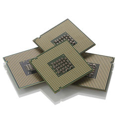
GS88132CGD-250I
SRAM Chip Sync Single 2.5V/3.3V 9M-Bit 256K x 32 5.5ns/2.5ns 165-Pin FBGA Tray
- RoHS 10 Compliant
- Tariff Charges
- IEEE 1149.1 JTAG-compatible Boundary Scan
- 2.5 V or 3.3 V +10%/–10% core power supply
- 2.5 V or 3.3 V I/O supply
- LBO pin for Linear or Interleaved Burst mode
- Internal input resistors on mode pins allow floating mode pins
- Byte Write (BW) and/or Global Write (GW) operation
- Internal self-timed write cycle
- Automatic power-down for portable applications
- JEDEC-standard 100-lead TQFP and 165-bump BGA packages
- RoHS-compliant 100-lead TQFP and 165-bump BGA packages available
Technical Attributes
Find Similar Parts
| Description | Value | |
|---|---|---|
| 17 Bit | ||
| Flow-Through|Pipelined | ||
| 250 MHz | ||
| SDR | ||
| 9 Mbit | ||
| Tin-Silver-Copper | ||
| 260 | ||
| 175@Flow-Through|215@Pipelined mA | ||
| 2.7, 3.6 V | ||
| 5.5@Flow-Through|2.5@Pipelined ns | ||
| 9 Mbit | ||
| 2.3, 3 V | ||
| Surface Mount | ||
| MSL 3 - 168 hours | ||
| 165 | ||
| 32 Bit | ||
| 32 Bit | ||
| 1 | ||
| 256 kWords | ||
| -40 to 85 °C | ||
| 85 °C | ||
| -40 °C | ||
| 165FBGA | ||
| 165 | ||
| 15 x 13 x 0.94 mm | ||
| No | ||
| Industrial | ||
| Synchronous SRAM | ||
| FBGA | ||
| 2.7, 3.6 V | ||
| 2.3, 3 V | ||
| 2.5, 3.3 V | ||
| Synchronous | ||
| 2.5, 3.3 V |
ECCN / UNSPSC / COO
| Description | Value |
|---|---|
| Country of Origin: | RECOVERY FEE |
| ECCN: | 3A991.B.2.B |
| HTSN: | 8542320041 |
| Schedule B: | 8542320040 |
