
GS880F32CGT-7.5IV
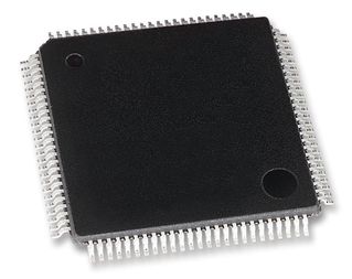
SRAM Chip Sync Quad 2.5V/3.3V 9M-Bit 256K x 32 7.5ns 100-Pin TQFP Bulk
-
 RoHS 10 Compliant
 -
 Tariff Charges
The GS880F32CGT is a 9,437,184-bit (8,388,608-bit for x32 version) high performance synchronous SRAM with a 2-bit burst address counter. Although of a type originally developed for Level 2 Cache applications supporting high performance CPUs, the device now finds application in synchronous SRAM applications, ranging from DSP main store to networking chip set support.Controls :Addresses, data I/Os, chip enables (E1, E2, E3), address burst control inputs (ADSP, ADSC, ADV), and write control inputs (Bx, BW, GW) are synchronous and are controlled by a positive-edge-triggered clock input (CK). Output enable (G) and power down control (ZZ) are asynchronous inputs. Burst cycles can be initiated with either ADSP or ADSC inputs. In Burst mode, subsequent burst addresses are generated internally and are controlled by ADV. The burst address counter may be configured to count in either linear or interleave order with the Linear Burst Order (LBO) input. The Burst function need not be used. New addresses can be loaded on every cycle with no degradation of chip performance.Designing For Compatibility :The JEDEC standard for Burst RAMS calls for a FT mode pin option on Pin 14. Board sites for flow through Burst RAMS should be designed with VSS connected to the FT pin location to ensure the broadest access to multiple vendor sources. Boards designed with FT pin pads tied low may be stuffed with GSI’s pipeline/flow through-configurable Burst RAMs or any vendor’s flow through or configurable Burst SRAM. Boards designed with the FT pin location tied high or floating must employ a non-configurable flow through Burst RAM, like this RAM, to achieve flow through functionality.Byte Write and Global Write :Byte write operation is performed by using Byte Write enable (BW) input combined with one or more individual byte write signals (Bx). In addition, Global Write (GW) is available for writing all bytes at one time, regardless of the Byte Write control inputs.Sleep Mode :Low power (Sleep m
- Flow Through mode operation; Pin 14 = No Connect
- 2.5 V or 3.3 V +10%/–10% core power supply
- 2.5 V or 3.3 V I/O supply
- LBO pin for Linear or Interleaved Burst mode
- Internal input resistors on mode pins allow floating mode pins
- Byte Write (BW) and/or Global Write (GW) operation
- Internal self-timed write cycle
- Automatic power-down for portable applications
- JEDEC-standard 100-lead TQFP package
- RoHS-compliant 100-lead TQFP package available
Technical Attributes
Find Similar Parts
| Description | Value | |
|---|---|---|
| 18 Bit | ||
| Flow-Through | ||
| SDR | ||
| 9 Mbit | ||
| 150 mA | ||
| 2.7, 3.6 V | ||
| 7.5 ns | ||
| 9 Mbit | ||
| 2.3, 3 V | ||
| Surface Mount | ||
| 100 | ||
| 32 Bit | ||
| 32 Bit | ||
| 4 | ||
| 256 kWords | ||
| -40 to 85 °C | ||
| 85 °C | ||
| -40 °C | ||
| 100TQFP | ||
| 100 | ||
| 14 x 20 x 1.4 mm | ||
| 0 | ||
| Industrial | ||
| Synchronous SRAM | ||
| TQFP | ||
| 2.7, 3.6 V | ||
| 2.3, 3 V | ||
| 2.5, 3.3 V | ||
| Synchronous | ||
| 2.5, 3.3 V |
ECCN / UNSPSC / COO
| Description | Value |
|---|---|
| Country of Origin: | RECOVERY FEE |
| ECCN: | 3A991.B.2.B |
| HTSN: | 8542320041 |
| Schedule B: | 8542320040 |