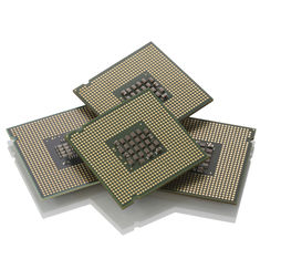
GS8342T08BD-333
SRAM Chip Sync Single 1.8V 36M-Bit 4M x 8 0.45ns 165-Pin FBGA
- RoHS 10 Compliant
- Tariff Charges
The GS8342T08 is a built in compliance with the -II SRAM pin out standard for Common I/O synchronous SRAMs. They are 37,748,736-bit (36Mb) SRAMs. The GS8342T08 -II SRAMs are just one element in a family of low power, low voltage HSTL I/O SRAMs designed to operate at the speeds needed to implement economical high performance networking systems.Clocking and Addressing Schemes: The GS8342T08 is a -II SRAMs are synchronous devices. They employ two input register clock inputs, K and K. K and K are independent single-ended clock inputs, not differential inputs to a single differential clock input buffer. The device also allows the user to manipulate the output register clock inputs quasi independently with the C and C clock inputs. C and C are also independent single-ended clock inputs, not differential inputs. If the C clocks are tied high, the K clocks are routed internally to fire the output registers instead.Each internal read and write operation in a -II B2 RAM is two times wider than the device I/O bus. An input data bus de-multiplexer is used to accumulate incoming data before it is simultaneously written to the memory array. An output data multiplexer is used to capture the data produced from a single memory array read and then route it to the appropriate output drivers as needed.When a new address is loaded into a x18 or x36 version of the part, A0 is used to initialize the pointers that control the data multiplexer / de-multiplexer so the RAM can perform critical word first" operations. From an external address point of view, regardless of the starting point, the data transfers always follow the same sequence {0, 1} or {1, 0} .Unlike the x18 and x36 versions, the input and output data multiplexers of the x8 and x9 versions are not pre-set by address inputs and therefore do not allow "critical word first" operations. The address fields of the x8 and x9 -II B2 RAMs are one address pin less than the advertised index depth (e.g., the 4M x 8 has a 2M addressable ind"
- Simultaneous Read and Write ™ Interface
- Common I/O bus
- JEDEC-standard pinout and package
- Double Data Rate interface
- Byte Write (x36, x18 and x9) and Nibble Write (x8) function
- Burst of 2 Read and Write
- 1.8 V +100/–100 mV core power supply
- 1.5 V or 1.8 V HSTL Interface
- Pipelined read operation with self-timed Late Write
- Fully coherent read and write pipelines
- ZQ pin for programmable output drive strength
- IEEE 1149.1 JTAG-compliant Boundary Scan
- Pin-compatible with present 9Mb, 18Mb, 36Mb and 72Mb devices
- 165-bump, 13 mm x 15 mm, 1 mm bump pitch BGA package
- RoHS-compliant 165-bump BGA package available
Technical Attributes
Find Similar Parts
| Description | Value | |
|---|---|---|
| 21 Bit | ||
| Pipelined | ||
| 333 MHz | ||
| DDR | ||
| 36 Mbit | ||
| 333 MHz | ||
| 515 mA | ||
| 0.45 ns | ||
| 36 Mbit | ||
| Surface Mount | ||
| 165 | ||
| 8 Bit | ||
| 8 Bit | ||
| 1 | ||
| 4 MWords | ||
| 0 to 85 °C | ||
| 85 °C | ||
| 0 °C | ||
| 165FBGA | ||
| 165 | ||
| 15 x 13 x 0.94 mm | ||
| No | ||
| Commercial | ||
| SigmaDDR SRAM | ||
| FBGA | ||
| 1.8 V | ||
| Synchronous | ||
| 1.8000 V |
ECCN / UNSPSC / COO
| Description | Value |
|---|---|
| Country of Origin: | RECOVERY FEE |
| ECCN: | 3A991.B.2.B |
| HTSN: | 8542320041 |
| Schedule B: | 8542320040 |
