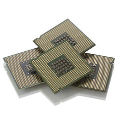
GS8342S36BD-400I
SRAM Chip Sync Dual 1.8V 36M-Bit 1M x 36 0.45ns 165-Pin FBGA
- RoHS 10 Compliant
- Tariff Charges
The GS8342S36BD is a built in compliance with the Sigma SIO DDR-II SRAM pin out standard for Separate I/O synchronous SRAMs. They are 37,748,736-bit (36Mb) SRAMs. These are the first in a family of wide, very low voltage HSTL I/O SRAMs designed to operate at the speeds needed to implement economical high performance networking systems.Clocking and Addressing Schemes: A Burst of 2 Sigma SIO DDR-II SRAM is a synchronous device. It employs dual input register clock inputs, K and K. The device also allows the user to manipulate the output register clock input quasi independently with dual output register clock inputs, C and C. If the C clocks are tied high, the K clocks are routed internally to fire the output registers instead. Each Burst of 2 Sigma SIO DDR-II SRAM also supplies Echo Clock outputs, CQ and CQ, which are synchronized with read data output. When used in a source synchronous clocking scheme, the Echo Clock outputs can be used to fire input registers at the data’s destination.Each internal read and write operation in a Sigma SIO DDR-II B2 RAM is two times wider than the device I/O bus. An input data bus de-multiplexer is used to accumulate incoming data before it is simultaneously written to the memory array. An output data multiplexer is used to capture the data produced from a single memory array read and then route it to the appropriate output drivers as needed. Therefore, the address field of a Sigma SIO DDR-II B2 is always one address pin less than the advertised index depth (e.g., the 4M x 8 has an 2M addressable index).
- Simultaneous Read and Write Sigma SIO™ Interface
- JEDEC-standard pinout and package
- Dual Double Data Rate interface
- Byte Write controls sampled at data-in time
- DLL circuitry for wide output data valid window and future frequency scaling
- Burst of 2 Read and Write
- 1.8 V +100/–100 mV core power supply
- 1.5 V or 1.8 V HSTL Interface
- Pipelined read operation
- Fully coherent read and write pipelines
- ZQ mode pin for programmable output drive strength
- IEEE 1149.1 JTAG-compliant Boundary Scan
- 3rd Generation, 165-bump, 13 mm x 15 mm, 1 mm bump pitch BGA package
- RoHS-compliant 165-bump BGA package available
Technical Attributes
Find Similar Parts
| Description | Value |
|---|
ECCN / UNSPSC / COO
| Description | Value |
|---|---|
| Country of Origin: | RECOVERY FEE |
| ECCN: | 3A991.B.2.B |
| HTSN: | 8542320041 |
| Schedule B: | 8542320040 |
