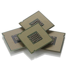
GS8342R18BGD-400I
SRAM Chip Sync Single 1.8V 36M-Bit 2M x 18 0.45ns 165-Pin FBGA
- RoHS 10 Compliant
- Tariff Charges
The GS8342R18 is a built in compliance with the -II SRAM pin out standard for Common I/O synchronous SRAMs. They are 37,748,736-bit (36Mb) SRAMs. The GS8342R18 -II SRAMs are just one element in a family of low power, low voltage HSTL I/O SRAMs designed to operate at the speeds needed to implement economical high performance networking systems.Clocking and Addressing Schemes: The GS8342R18 -II SRAMs are synchronous devices. They employ two input register clock inputs, K and K. K and K are independent single-ended clock inputs, not differential inputs to a single differential clock input buffer. The device also allows the user to manipulate the output register clock inputs quasi independently with the C and C clock inputs. C and C are also independent single-ended clock inputs, not differential inputs. If the C clocks are tied high, the K clocks are routed internally to fire the output registers instead.Each internal read and write operation in a -II B4 RAM is four times wider than the device I/O bus. An input data bus de-multiplexer is used to accumulate incoming data before it is simultaneously written to the memory array. An output data multiplexer is used to capture the data produced from a single memory array read and then route it to the appropriate output drivers as needed.When a new address is loaded into a x18 or x36 version of the part, A0 and A1 are used to initialize the pointers that control the data multiplexer / de-multiplexer so the RAM can perform critical word first" operations. From an external address point of view, regardless of the starting point, the data transfers always follow the same linear sequence {00, 01, 10, 11} or {01, 10, 11, 00} or {10, 11, 00, 01} or {11, 00, 01, 10} .Unlike the x18 and x36 versions, the input and output data multiplexers of the x8 and x9 versions are not pre-set by address inputs and therefore do not allow "critical word first" operations. The address fields of the x8 and x9 -II B4 RAMs are two address pins less th"
- Simultaneous Read and Write ™ Interface
- Common I/O bus
- JEDEC-standard pinout and package
- Double Data Rate interface
- Byte Write (x36, x18 and x9) and Nibble Write (x8) function
- Burst of 4 Read and Write
- 1.8 V +100/–100 mV core power supply
- 1.5 V or 1.8 V HSTL Interface
- Pipelined read operation with self-timed Late Write
- Fully coherent read and write pipelines
- ZQ pin for programmable output drive strength
- IEEE 1149.1 JTAG-compliant Boundary Scan
- Pin-compatible with present 9Mb, 18Mb, 36Mb and 72Mb devices
- RoHS-compliant 165-bump BGA package available
- 3rd Generation, Green 13 mm x 15 mm, 165 FPBGA
Technical Attributes
Find Similar Parts
| Description | Value | |
|---|---|---|
| 21 Bit | ||
| Pipelined | ||
| 400 MHz | ||
| DDR | ||
| 36 Mbit | ||
| 400 MHz | ||
| 610 mA | ||
| 0.45 ns | ||
| 36 Mbit | ||
| Surface Mount | ||
| 165 | ||
| 18 Bit | ||
| 18 Bit | ||
| 1 | ||
| 2 MWords | ||
| -40 to 100 °C | ||
| 100 °C | ||
| -40 °C | ||
| 165FBGA | ||
| 165 | ||
| 15 x 13 x 0.94 mm | ||
| No | ||
| Industrial | ||
| SigmaDDR SRAM | ||
| FBGA | ||
| 1.8 V | ||
| Synchronous | ||
| 1.8000 V |
ECCN / UNSPSC / COO
| Description | Value |
|---|---|
| Country of Origin: | RECOVERY FEE |
| ECCN: | 3A991.B.2.B |
| HTSN: | 8542320041 |
| Schedule B: | 8542320040 |
