
GS8320E32AGT-250V
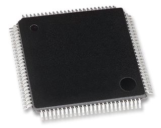
SRAM Chip Sync Quad 1.8V/2.5V 36M-Bit 1M x 32 5.5ns 100-Pin TQFP Bulk
-
 RoHS 10 Compliant
 -
 Tariff Charges
The GS8320E32AGT is a 37,748,736-bit high performance synchronous SRAM with a 2-bit burst address counter. Although of a type originally developed for Level 2 Cache applications supporting high performance CPUs, the device now finds application in synchronous SRAM applications, ranging from DSP main store to networking chip set support.Controls :Addresses, data I/Os, chip enables (E1, E2, E3), address burst control inputs (ADSP, ADSC, ADV), and write control inputs (Bx, BW, GW) are synchronous and are controlled by a positive-edge-triggered clock input (CK). Output enable (G) and power down control (ZZ) are asynchronous inputs. Burst cycles can be initiated with either ADSP or ADSC inputs. In Burst mode, subsequent burst addresses are generated internally and are controlled by ADV. The burst address counter may be configured to count in either linear or interleave order with the Linear Burst Order (LBO) input. The Burst function need not be used. New addresses can be loaded on every cycle with no degradation of chip performance.DCD Pipelined Reads :The GS8320E32AGT is a DCD (Dual Cycle Deselect) pipelined synchronous SRAM. SCD (Single Cycle Deselect) versions are also available. DCD SRAMs pipeline disable commands to the same degree as read commands. DCD RAMs hold the deselect command for one full cycle and then begin turning off their outputs just after the second rising edge of clock.Byte Write and Global Write :Byte write operation is performed by using Byte Write enable (BW) input combined with one or more individual byte write signals (Bx). In addition, Global Write (GW) is available for writing all bytes at one time, regardless of the Byte Write control inputs.Sleep Mode :Low power (Sleep mode) is attained through the assertion (High) of the ZZ signal, or by stopping the clock (CK). Memory data is retained during Sleep mode.Core and Interface Voltages :The GS8320E32AGT operates on a 1.8 V or 2.5 V power supply. All inputs are 1.8 V or 2.5 V compatible. Separat
- FT pin for user-configurable flow through or pipeline operation
- Single Dual Cycle Deselect (SDCD) operation
- 1.8 V or 2.5 V core power supply
- 1.8 V or 2.5 V I/O supply
- LBO pin for Linear or Interleaved Burst mode
- Internal input resistors on mode pins allow floating mode pins
- Byte Write (BW) and/or Global Write (GW) operation
- Internal self-timed write cycle
- Automatic power-down for portable applications
- RoHS-compliant 100-lead TQFP package available
Technical Attributes
Find Similar Parts
| Description | Value |
|---|
ECCN / UNSPSC / COO
| Description | Value |
|---|---|
| Country of Origin: | RECOVERY FEE |
| ECCN: | 3A991.B.2.B |
| HTSN: | 8542320041 |
| Schedule B: | 8542320040 |