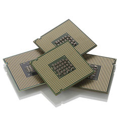
GS8182Q18BGD-250I
SRAM Chip Sync Dual 1.8V 18M-Bit 1M x 18 0.45ns 165-Pin FBGA Tray
- RoHS 10 Compliant
- Tariff Charges
The GS8182Q18BGD are built in compliance with the Sigma Quad-II SRAM pin out standard for Separate I/O synchronous SRAMs. They are 18,874,368-bit (18Mb) SRAMs. The GS8182Q18BGD Sigma Quad SRAMs are just one element in a family of low power, low voltage HSTL I/O SRAMs designed to operate at the speeds needed to implement economical high performance networking systems.
- Simultaneous Read and Write Sigma Quad™ Interface
- JEDEC-standard pin out and package
- Dual Double Data Rate interface
- Byte Write controls sampled at data-in time
- Burst of 2 Read and Write
- 1.8 V +100/–100 mV core power supply
- 1.5 V or 1.8 V HSTL Interface
- Pipelined read operation
- Fully coherent read and write pipelines
- ZQ pin for programmable output drive strength
- IEEE 1149.1 JTAG-compliant Boundary Scan
- Pin-compatible with present 9Mb and future 36Mb and 144Mb devices
- 3rd Generation
- Green 13 mm x 15 mm, 165 FPBGA
- RoHS-compliant 165-bump BGA package available
- 1MB product Family
- Default to SCD x18 Interleaved Pipeline mode
Technical Attributes
Find Similar Parts
| Description | Value | |
|---|---|---|
| 19 Bit | ||
| Pipelined | ||
| 250 MHz | ||
| DDR | ||
| 18 Mbit | ||
| Tin-Silver-Copper | ||
| 260 | ||
| 250 MHz | ||
| 605 mA | ||
| 0.45 ns | ||
| 1M x 18bit | ||
| 18 Mbit | ||
| Surface Mount | ||
| MSL 3 - 168 hours | ||
| 165 | ||
| 18 Bit | ||
| 18 Bit | ||
| 2 | ||
| 1 MWords | ||
| -40 to 85 °C | ||
| 85 °C | ||
| -40 °C | ||
| 165FBGA | ||
| 165 | ||
| 15 x 13 x 0.94 mm | ||
| No | ||
| Industrial | ||
| SigmaQuad SRAM | ||
| FBGA | ||
| 1.8 V | ||
| Synchronous | ||
| 1.8000 V |
ECCN / UNSPSC / COO
| Description | Value |
|---|---|
| Country of Origin: | RECOVERY FEE |
| ECCN: | 3A991.B.2.B |
| HTSN: | 8542320041 |
| Schedule B: | 8542320040 |
