
PI6C2408-3WEX
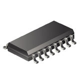
Zero Delay PLL Clock Multiplier Single 16-Pin SOIC T/R
-
 RoHS 10 Compliant
 -
 Tariff Charges

The PI6C2408 is a PLL-based, zero-delay buffer, with the ability to distribute eight outputs of up to 140 MHz at 3.3 V. Two banks of four outputs exist, and, depending on product option ordered, can supply either reference frequency, prescaled half frequency, or multiplied 2x or 4x input clock frequencies. The PI6C2408 family has a power-sparing feature: when input SEL2 is 0, the component will 3-state one or both banks of outputs depending on the state of input SEL1. A PLL bypass test mode also exists. This product line is available in high-drive and industrial environment versions.An external feedback pin is used to synchronize the outputs to the input; the relationship between loading of this signal and the other outputs determines the input-output delay
- Maximum rated frequency: 140 MHz
- Low cycle-to-cycle jitter
- Input to output delay, less than 150ps
- External feedback pin allows outputs to be synchronized to the clock input
- 5V tolerant CLKIN input
- Operates at 3.3V VDD
- Test mode allows bypass of the PLL for system testing purposes (e.g., IBIS measurements)
- Clock frequency multipliers ½x to 4x dependent on option
- Packaging (Pb-free and Green available):
- 16-pin, 150-mil SOIC (W)
- 16-pin 173-mil TSSOP (L)
Technical Attributes
Find Similar Parts
| Description | Value |
|---|
ECCN / UNSPSC / COO
| Description | Value |
|---|---|
| Country of Origin: | RECOVERY FEE |
| ECCN: | EAR99 |
| HTSN: | 8542330001 |
| Schedule B: | 8542330000 |
 Factory Lead Time: