
XC7K325T-L2FFG900E
FPGA Kintex-7 Family 326080 Cells 28nm Technology 1V 900-Pin FC-BGA
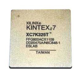
Click image to enlarge
Manufacturer:AMD
Product Category:
Programmable Logic, FPGAs
Avnet Manufacturer Part #: XC7K325T-L2FFG900E
Secondary Manufacturer Part#: XC7K325T-L2FFG900E
-
 RoHS 10 Compliant
 -
 Tariff Charges
XC7K325T-L2FFG900E is a Kintex®-7 FPGA IC. It addresses the complete range of system requirements, ranging from low-cost, small form factors, cost-sensitive, high-volume applications to ultra-high-end connectivity bandwidth, logic capacity, and signal processing capability for the most demanding high-performance applications. It is optimized for best price performance with a 2X improvement compared to the previous generation, enabling a new class of FPGAs.
- 36Kb dual-port block RAM with built-in FIFO logic for on-chip data buffering
- Integrated block for PCI Express® (PCIe), for up to x8 Gen3 endpoint and root port designs
- 12.5Gb/s transceiver speed, 800Gb/s serial bandwidth
- x8 Gen2 PCIe interface, 1,866Mb/s memory interface
- 1.2V to 3.3V I/O voltage
- 326,080 logic cells
- 50,950 slices, 4,000KB max distributed RAM configurable logic blocks (CLBs)
- 890 (18KB), 445 (36KB), 16,020 max (KB) block RAM blocks
- 900-pin FCBGA package
- Extended temperature range from 0 to 100°C
Technical Attributes
Find Similar Parts
| Description | Value | |
|---|---|---|
| FCBGA | ||
| Surface Mount | ||
| 326, 80 | ||
| 900 | ||
| 350 | ||
| 100 °C | ||
| 0 °C | ||
| 28nm (HKMG) | ||
| Kintex-7 XC7K325T |
ECCN / UNSPSC / COO
| Description | Value |
|---|---|
| Country of Origin: | RECOVERY FEE |
| ECCN: | 3A991.D |
| HTSN: | 8542390090 |
| Schedule B: | 8542390060 |