
AS8C803601-QC150N
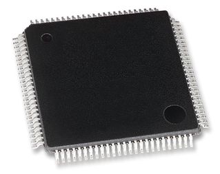
SRAM Chip Sync Dual 3.3V 9M-Bit 256K x 36 3.8ns 100-Pin TQFP
-
 RoHS 10 Compliant
 -
 Tariff Charges
The AS8C803601 is a 3.3V high-speed 9,437,184 bit (9 Megabit) synchronous SRAM. It is designed to eliminate dead bus cycles when turning the bus around between reads and writes, or writes and reads. Thus, it has been given the name ZBTTM, or Zero Bus Turnaround. Address and control signals are applied to the SRAM during one clock cycle, and two cycles later the associated data cycle occurs, be it read or write.The AS8C803601 contain data I/O, address and control signal registers. Output enable is the only asynchronous signal and can be used to disable the outputs at any given time.A Clock Enable( CEN) pin allows operation of the to AS8C803601 be suspended as long as necessary. All synchronous inputs are ignored when (CEN)is high and the internal device registers will hold their previous values. There are three chip enable pins (CE1, CE2, CE2) that allow the user to deselect the device when desired. If any one of these three are notasserted when ADV/LD is low, no new memory operation can be initiated. However, any pending data transfers (reads or writes) will be completed. The data bus will tri-state two cycles after chip is deselected or a write is initiated. TheAS8C803601 has an on-chip burst counter. In the burst mode,the AS8C803601 can provide fourcycles of data for a single address presented to the SRAM. The order of the burst sequence is defined by the LBO input pin. The LBO pin selects between linear and interleaved burst sequence. The ADV/LD signal is used to load a new external address (ADV/LD = LOW) or increment the internal burst counter (ADV/LD = HIGH).The AS8C803601 SRAM utilize IDT's latest high-performance CMOS process, and are packaged in a JEDEC Standard 14mm x 20mm 100- pin thin plastic quad flatpack (TQFP).
- 256K x 36, 512K x 18 memory configurations
- Supports high performance system speed - 150MHz (3.8ns Clock-to-Data Access)
- ZBTTM Feature - No dead cycles between write and read cycles
- Internally synchronized output buffer enable eliminates the need to control OE
- Single R/W (READ/WRITE) control pin
- Positive clock-edge triggered address, data, and control signal registers for fully pipelined applications
- 4-word burst capability (interleaved or linear)
- Individual byte write (BW1 - BW4) control (May tie active)
- Three chip enables for simple depth expansion
- 3.3V power supply (±5%)
- 3.3V I/O Supply (V DDQ)
- Power down controlled by ZZ input
- Packaged in a JEDEC standard 100-pin plastic thin quad flatpack (TQFP)
Technical Attributes
Find Similar Parts
| Description | Value |
|---|
ECCN / UNSPSC / COO
| Description | Value |
|---|---|
| Country of Origin: | RECOVERY FEE |
| ECCN: | EAR99 |
| HTSN: | 8542320041 |
| Schedule B: | 8542320040 |