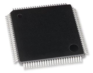
AS8C161831-QC166N
SRAM Chip Sync Dual 2.5V 18M-Bit 1M x 18 3.5ns 100-Pin TQFP
- RoHS 10 Compliant
- Tariff Charges
The AS8C161831 is a 2.5V high-speed 18,874,368-bit (18 Megabit) synchronous SRAMs . It is designed to eliminate dead bus cycles when turning the bus around between reads and writes, or writes and reads. Thus, it has been given the name ZBP', or Zero Bus Turnaround Address and control signals are applied to the SRAM during one clack cycle, and two cycles later the associated data cycle occurs, be it read or write.The AS8C161831 contain data I/O, address and control signal registers Output enable is the only asynchronous signal and can be used to disable the outputs at any given time.A Clock Enable CEN pin allows operation of the AS8C161831 to be suspended as long as necessary All synchronous inputs are ignored when (CEN) is high and the internal device registers will hold their previous values.There are three chip enable pins (CE.), CE2, CE2) that allow the user to deselect the device when desired If any one of these three is not asserted when ADV/LD is low, no new memory operation can be initiated.
- 512K x 36, 1M x 18 memory configurations
- Supports high performance system speed - 200 MHz (3 2 ns Clock-to-Data Access)
- ZBTTM Feature - No dead cycles between write and read cycles
- Internally synchronized output buffer enable eliminates the need to control OE
- Single Ra (READ/WAITE) control pin
- Positive clock-edge triggered address, data, and control signal registers for fully pipelined applications
- 4-word burst capability (interleaved or linear)
- Individual byte write (BM - BW4) control (May tie active)
- Three chip enables for simple depth expansion
- 2 5V power supply (-_t5%)
- 2 5V I/O Supply (V000)
- Power down controlled by ZZ input
- Boundary Scan JTAG Interface (IEEE 1149 1 Compliant)
- Packaged in a JEDEC standard 100-pin plastic thin quad flatpack (TQFP)
Technical Attributes
Find Similar Parts
| Description | Value | |
|---|---|---|
| 20 Bit | ||
| Pipelined | ||
| 166 MHz | ||
| SDR | ||
| 18 Mbit | ||
| 166 MHz | ||
| 245 mA | ||
| 3.5 ns | ||
| 18 Mbit | ||
| Surface Mount | ||
| 100 | ||
| 18 Bit | ||
| 18 Bit | ||
| 2 | ||
| 1 MWords | ||
| 0 to 70 °C | ||
| 70 °C | ||
| 0 °C | ||
| 100TQFP | ||
| 100 | ||
| 20.2 x 14.2 x 1.45 mm | ||
| No | ||
| Commercial | ||
| Synchronous SRAM | ||
| TQFP | ||
| 2.5 V | ||
| Synchronous | ||
| 2.5000 V |
ECCN / UNSPSC / COO
| Description | Value |
|---|---|
| Country of Origin: | RECOVERY FEE |
| ECCN: | EAR99 |
| HTSN: | 8542320041 |
| Schedule B: | 8542320040 |
