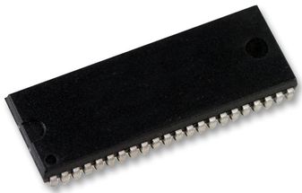
AS7C31026B-15JCN
SRAM Chip Async Single 3.3V 1M-Bit 64K x 16 15ns 44-Pin SOJ
- RoHS 10 Compliant
- Tariff Charges
The AS7C31026B is a high-performance CMOS 1,048,576-bit Static Random Access Memory (SRAM) device organized as 65,536 words × 16 bits. It is designed for memory applications where fast data access, low power, and simple interfacing are desired. Equal address access and cycle times (tAA, tRC, tWC) of 10/12/15/20 ns with output enable access times (tOE) of 5, 6, 7, 8 ns are ideal for high-performance applications.When CE is high, the device enters standby mode. A write cycle is accomplished by asserting write enable (WE) and chip enable (CE). Data on the input pins I/O0 through I/O15 is written on the rising edge of WE (write cycle 1) or CE (write cycle 2). To avoid bus contention, external devices should drive I/O pins only after outputs have been disabled with output enable (OE) or write enable (WE). A read cycle is accomplished by asserting output enable (OE) and chip enable (CE) with write enable (WE) high. The chips drive I/O pins with the data word referenced by the input address. When either chip enable or output enable is inactive or write enable is active, output drivers stay in high-impedance mode.The device provides multiple center power and ground pins, and separate byte enable controls, allowing individual bytes to be written and read. LB controls the lower bits, I/O0 through I/O7, and UB controls the higher bits, I/O8 through I/O15. All chip inputs and outputs are TTL-compatible, and operation is from a single 3.3 V supply. The device is packaged in common industry standard packages.
- Industrial and commercial versions
- Organization: 65,536 words × 16 bits
- Center power and ground pins for low noise
- High speed
- 10/12/15/20 ns address access time
- 5, 6, 7, 8 ns output enable access time
- Low power consumption: ACTIVE
- 288 mW / max @ 10 ns
- Low power consumption: STANDBY
- 18 mW / max CMOS I/O
- 6 T 0.18 u CMOS technology
- Easy memory expansion with CE, OE inputs
- TTL-compatible, three-state I/O
- JEDEC standard packaging
- 44-pin 400 mil SOJ
- 44-pin TSOP 2-400
- ESD protection = 2000 volts
- Latch-up current = 200 mA
Technical Attributes
Find Similar Parts
| Description | Value | |
|---|---|---|
| 16 Bit | ||
| 1 Mbit | ||
| 70 mA | ||
| 15 ns | ||
| 1 Kb | ||
| Surface Mount | ||
| 44 | ||
| 16 Bit | ||
| 16 Bit | ||
| 1 | ||
| 64 kWords | ||
| 0 to 70 °C | ||
| 70 °C | ||
| 0 °C | ||
| 44SOJ | ||
| 44 | ||
| 28.7 x 10.29 x 2.92 mm | ||
| No | ||
| Commercial | ||
| CMOS SRAM | ||
| SOJ | ||
| 3.3 V | ||
| Asynchronous | ||
| 3.3000 V |
ECCN / UNSPSC / COO
| Description | Value |
|---|---|
| Country of Origin: | RECOVERY FEE |
| ECCN: | EAR99 |
| HTSN: | 8542320041 |
| Schedule B: | 8542320040 |
