
AS7C1024B-12TJIN
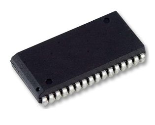
SRAM, 1 Mbit, 128K x 8bit, 5V, 32-Pin, SOJ
-
 RoHS 10 Compliant
 -
 Tariff Charges
The AS7C1024B is a high performance CMOS 1,048,576-bit Static Random Access Memory (SRAM) device organized as 131,072 words x 8 bits. It is designed for memory applications where fast data access, low power, and simple interfacing are desired. Equal address access and cycle times (tAA, tRC, tWC) of 10/12/15/20 ns with output enable access times (tOE) of 5/6/7/8 ns are ideal for high performance applications. Active high and low chip enables (CE1, CE2) permit easy memory expansion with multiple-bank systems. When CE1 is high or CE2 is low, the devices enter standby mode. If inputs are still toggling, the device will consume ISB power. If the bus is static, then full standby power is reached (ISB1). For example, the AS7C1024B is guaranteed not to exceed 55 mW under nominal full standby conditions.A write cycle is accomplished by asserting write enable (WE) and both chip enables (CE1, CE2). Data on the input pins I/O0 through I/O7 is written on the rising edge of WE (write cycle 1) or the active-to-inactive edge of CE1 or CE2 (write cycle 2). To avoid bus contention, external devices should drive I/O pins only after outputs have been disabled with output enable (OE) or write enable (WE). A read cycle is accomplished by asserting output enable (OE) and both chip enables (CE1, CE2), with write enable (WE) high. The chips drive I/ O pins with the data word referenced by the input address. When either chip enable is inactive, output enable is inactive, or write enable is active, output drivers stay in high-impedance mode.
- Industrial and commercial temperatures
- Organization: 131,072 words x 8 bits
- High speed
- 10/12/15/20 ns address access time
- 5/6/7/8 ns output enable access time
- Low power consumption: ACTIVE
- 605 mW / max @ 10 ns
- Low power consumption: STANDBY
- 55 mW / max CMOS
- 6T 0.18u CMOS technology
- Easy memory expansion with CE1, CE2, OE inputs
- TTL/LVTTL-compatible, three-state I/O
- 32-pin JEDEC standard packages
- 300 mil SOJ
- 400 mil SOJ
- 8 × 20mm TSOP 1
- 8 x 13.4mm sTSOP 1
- ESD protection = 2000 volts
- Latch-up current = 200 mA
Technical Attributes
Find Similar Parts
| Description | Value | |
|---|---|---|
| 17 Bit | ||
| 1 Mbit | ||
| 100 mA | ||
| 12 ns | ||
| 128K x 8bit | ||
| 1 Kb | ||
| Surface Mount | ||
| 32 | ||
| 8 Bit | ||
| 8 Bit | ||
| 1 | ||
| 128 kWords | ||
| 0 to 70 °C | ||
| 70 °C | ||
| 0 °C | ||
| 32SOJ | ||
| 32 | ||
| 21.08 x 7.75 x 2.67 mm | ||
| AS7C1024B Series | ||
| No | ||
| Commercial | ||
| CMOS SRAM | ||
| SOJ | ||
| 5.5 V | ||
| 4.5 V | ||
| 5 V | ||
| Asynchronous | ||
| 5.0000 V |
ECCN / UNSPSC / COO
| Description | Value |
|---|---|
| Country of Origin: | RECOVERY FEE |
| ECCN: | EAR99 |
| HTSN: | 8542320041 |
| Schedule B: | 8542320040 |