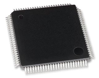
制造商:
ISSI
IS64LPS12832A-200TQLA3
SRAM Chip Sync Quad 3.3V 4M-Bit 128K x 32 3.1ns 100-Pin TQFP
安富利制造商模型#:
IS64LPS12832A-200TQLA3
RoHS 6 Compliant
The IS64LPS12832A are high-speed, low-power synchronous static RAMs designed to provide burstable, high-performance memory for communication and networking applications. The IS64LPS12832A is organized as 131,072 words by 32 bits. Fabricated with advanced CMOS technology, the device integrates a 2-bit burst counter, high-speed SRAM core, and high-drive capability outputs into a single monolithic circuit. All synchronous inputs pass through registers controlled by a positive-edge-triggered single clock input. Write cycles are internally self-timed and are initiated by the rising edge of the clock input. Write cycles can be one to four bytes wide as controlled by the write control inputs. Separate byte enables allow individual bytes to be written. The byte write operation is performed by using the byte write enable (BWE\) input combined with one or more individual byte write signals (BWX\). In addition, Global Write (GW\) is available for writing all bytes at one time, regardless of the byte write controls. Bursts can be initiated with either ADSP\ (Address Status Processor) or ADSC\ (Address Status Cache Controller) input pins. Subsequent burst addresses can be generated internally and controlled by the ADV\ (burst address advance) input pin. The mode pin is used to select the burst sequence order, Linear burst is achieved when this pin is tied LOW. Interleave burst is achieved when this pin is tied HIGH or left floating.
技术参数
- Internal self-timed write cycle
- Individual Byte Write Control and Global Write
- Clock controlled, registered address, data and control
- Burst sequence control using MODE input
- Three chip enable option for simple depth expansion and address pipelining
- Common data inputs and data outputs
- Auto Power-down during deselect
- Single cycle deselect
- Snooze MODE for reduced-power standby
- Power Supply: Vdd 3.3V + 5%, Vddq 3.3V/2.5V + 5%
- JEDEC 100-Pin QFP, 119-ball and 165-ball BGA packages
- Automotive available
- Lead Free available.
技术特性
查找类似的料号|
|
描述 | 值 |
|---|---|---|
|
|
最高工作温度 | 125 °C |
|
|
时钟频率最大值 | 200 MHz |
|
|
存储密度 | 4 Mbit |
|
|
额定电源电压 | 3.3 V |
|
|
集成电路安装 | Surface Mount |
|
|
引脚数 | 100 |
|
|
最低工作温度 | -40 °C |
|
|
最大电源电压 | 3.465 V |
|
|
SRAM类型 | SDR |
|
|
最小电源电压 | 3.135 V |
|
|
集成电路外壳/封装 | TQFP |
ECCN / UNSPSC
| 描述 | 值 |
|---|---|
| ECCN: | EAR99 |
| 计划交货期 B: | 8542320040 |
| HTSN: | 8542320041 |

