制造商:
ISSI
IS61NLP51218A-200TQLI
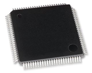
SRAM Chip Sync Dual 3.3V 9M-Bit 512K x 18 3.1ns 100-Pin TQFP
安富利制造商模型#:
IS61NLP51218A-200TQLI-TR
RoHS 6 Compliant
The 9 Meg 'NLP/NVP' product family feature high-speed, low-power synchronous static RAMs designed to provide a burstable, high-performance, 'no wait' state, device for networking and communications applications. They are organized as 256K words by 36 bits and 512K words by 18 bits, fabricated with ISSI's advanced CMOS technology. Incorporating a 'no wait' state feature, wait cycles are eliminated when the bus switches from read to write, or write to read. This device integrates a 2-bit burst counter, high-speed SRAM core, and high-drive capability outputs into a single monolithic circuit. All synchronous inputs pass through registers are controlled by a positive-edge-triggered single clock input. Operations may be suspended and all synchronous inputs ignored when Clock Enable, CKE is HIGH. In this state the internal device will hold their previous values. All Read, Write and Deselect cycles are initiated by the ADV input. When the ADV is HIGH the internal burst counter is incremented. New external addresses can be loaded when ADV is LOW. Write cycles are internally self-timed and are initiated by the rising edge of the clock inputs and when WE is LOW. Separate byte enables allow individual bytes to be written. A burst mode pin (MODE) defines the order of the burst sequence. When tied HIGH, the inter leaved burst sequence is selected. When tied LOW, the linear burst sequence is selected.
技术参数
- 100 percent bus utilization
- No wait cycles between Read and Write
- Internal self-timed write cycle
- Individual Byte Write Control
- Single R/W (Read/Write) control pin
- Clock controlled, registered address, data and control
- Interleaved or linear burst sequence control using MODE input
- Three chip enables for simple depth expansion and address pipelining
- Power Down mode
- Common data inputs and data outputs
- CKE pin to enable clock and suspend operation
- JEDEC 100-pin TQFP, 165-ball PBGA and 119-ball PBGA packages
- Power supply:
- NVP: Vdd 2.5V (± 5%), Vddq 2.5V (± 5%)
- NLP: Vdd 3.3V (± 5%), Vddq 3.3V/2.5V (± 5%)
- JTAG Boundary Scan for PBGA packages
- Industrial temperature available
- Lead-free available
技术特性
查找类似的料号|
|
描述 | 值 |
|---|---|---|
|
|
集成电路外壳/封装 | TQFP |
|
|
集成电路安装 | Surface Mount |
|
|
引脚数 | 100 |
|
|
最大电源电压 | 3.465 V |
|
|
时钟频率最大值 | 200 MHz |
|
|
最小电源电压 | 3.135 V |
|
|
额定电源电压 | 3.3 V |
|
|
最高工作温度 | 85 °C |
|
|
最低工作温度 | -40 °C |
|
|
SRAM类型 | SDR |
|
|
存储密度 | 9 Mbit |
ECCN / UNSPSC
| 描述 | 值 |
|---|---|
| ECCN: | 3A991.b.2.a |
| 计划交货期 B: | PARTS... |
| HTSN: | PARTS... |

