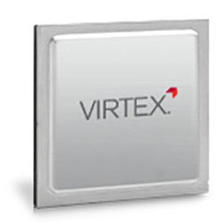
XC5VLX110-1FFG676I
FPGA Virtex-5 LX Family 110592 Cells 65nm (CMOS) Technology 1V 676-Pin FCBGA
The Virtex®-5 family provides the newest most powerful features in the FPGA market. Using the second generation ASMBL (Advanced Silicon Modular Block) column-based architecture, the Virtex-5 family contains five distinct platforms (sub-families), the most choice offered by any FPGA family. Each platform contains a different ratio of features to address the needs of a wide variety of advanced logic designs. In addition to the most advanced, high-performance logic fabric, Virtex-5 FPGAs contain many hard-IP system level blocks, including powerful 36-Kbit block RAM/FIFOs, second generation 25 x 18 DSP slices, SelectIO technology with built-in digitallycontrolled impedance, ChipSync source-synchronous interface blocks, system monitor functionality, enhanced clock management tiles with integrated DCM (Digital Clock Managers) and phase-locked-loop (PLL) clock generators, and advanced configuration options. Additional platform dependant features include power-optimized high-speed serial transceiver blocks for enhanced serial connectivity, PCI Express® compliant integrated Endpoint blocks, tri-mode Ethernet MACs (Media Access Controllers), and high-performance PowerPC® 440 microprocessor embedded blocks. These features allow advanced logic designers to build the highest levels of performance and functionality into their FPGA-based systems. Built on a 65-nm state-of-the-art copper process technology, Virtex-5 FPGAs are a programmable alternative to custom ASIC technology. Most advanced system designs require the programmable strength of FPGAs. Virtex-5 FPGAs offer the best solution for addressing the needs of high-performance logic designers, high-performance DSP designers, and high-performance embedded systems designers with unprecedented logic, DSP, hard/soft microprocessor, and connectivity capabilities. The Virtex-5 LX platform include advanced high-speed serial connectivity and link/transaction layer capability.
技術參數
- Five platforms LX, LXT, SXT, TXT, and FXT
- Virtex-5 LX: High-performance general logic applications
- Virtex-5 LXT: High-performance logic with advanced serial connectivity
- Virtex-5 SXT: High-performance signal processing applications with advanced serial connectivity
- Virtex-5 TXT: High-performance systems with double density advanced serial connectivity
- Virtex-5 FXT: High-performance embedded systems with advanced serial connectivity
- Cross-platform compatibility
- LXT, SXT, and FXT devices are footprint compatible in the same package using adjustable voltage regulators
- Most advanced, high-performance, optimal-utilization, FPGA fabric
- Real 6-input look-up table (LUT) technology
- Dual 5-LUT option
- Improved reduced-hop routing
- 64-bit distributed RAM option
- SRL32/Dual SRL16 option
- Powerful clock management tile (CMT) clocking
- Digital Clock Manager (DCM) blocks for zero delay buffering, frequency synthesis, and clock phase shifting
- PLL blocks for input jitter filtering, zero delay buffering, frequency synthesis, and phase-matched clock division
- 36-Kbit block RAM/FIFOs
- True dual-port RAM blocks
- Enhanced optional programmable FIFO logic
- Programmable
- True dual-port widths up to x36
- Simple dual-port widths up to x72
- Built-in optional error-correction circuitry
- Optionally program each block as two independent 18-Kbit blocks
- High-performance parallel SelectIO technology
- 1.2 to 3.3V I/O Operation
- Source-synchronous interfacing using ChipSync™ technology
- Digitally-controlled impedance (DCI) active termination
- Flexible fine-grained I/O banking
- High-speed memory interface support
- Advanced DSP48E slices
- 25 x 18, two’s complement, multiplication
- Optional adder, subtracter, and accumulator
- Optional pipelining
- Optional bitwise logical functionality
- Dedicated cascade connections
- Flexible configuration options
- SPI and Parallel FLASH interface
- Multi-bitstream support with dedicated fallback reconfiguration logic
- Auto bus width detection capability
- System Monitoring capability on all devices
- On-chip/Off-chip thermal monitoring
- On-chip/Off-chip power supply monitoring
- JTAG access to all monitored quantities
- Integrated Endpoint blocks for PCI Express Designs
- LXT, SXT, TXT, and FXT Platforms
- Compliant with the PCI Express Base Specification 1.1
- x1, x4, or x8 lane support per block
- Works in conjunction with RocketIO™ transceivers
- Tri-mode 10/100/1000 Mb/s Ethernet MACs
- LXT, SXT, TXT, and FXT Platforms
- RocketIO transceivers can be used as PHY or connect to external PHY using many soft MII (Media Independent Interface) options
- RocketIO GTP transceivers 100 Mb/s to 3.75 Gb/s
- LXT and SXT Platforms
- RocketIO GTX transceivers 150 Mb/s to 6.5 Gb/s
- TXT and FXT Platforms
- PowerPC 440 Microprocessors
- FXT Platform only
- RISC architecture
- 7-stage pipeline
- 32-Kbyte instruction and data caches included
- Optimized processor interface structure (crossbar)
- 65-nm copper CMOS process technology
- 1.0V core voltage
- High signal-integrity flip-chip packaging available in standard or Pb-free package options
技術屬性
查找類似的料號|
|
描述 | 值 |
|---|---|---|
|
|
速度等級 | 1 |
|
|
最低工作溫度 | -40 |
|
|
集成電路貼裝 | Surface Mount |
|
|
用戶輸入/輸出數量 | 440 |
|
|
邏輯單元數量 | 110 |
|
|
引腳數 | 676 |
|
|
最高工作溫度 | 100 |
|
|
集成電路外殼/封裝 | FCBGA |
ECCN/UNSPSC
| 描述 | 值 |
|---|---|
| ECCN: | 3A991.d |
| 計劃交貨期 B: | PARTS... |
| HTSN: | PARTS... |
文件
文檔
| 標題 | 下載 | 類別 | 發布日期 |
|---|---|---|---|
| Virtex-5 FPGA Packaging and Pinout Specification | Technical-Specifications | 20130331 | |
| Functional Description of the Virtex-5 FPGA Architecture | User-Guides | 20130331 | |
| Virtex-5 Family Overview | Product-Guides | 20130331 |

