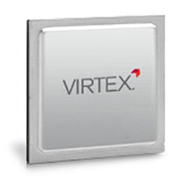
XC4VFX60-10FFG1152C
FPGA Virtex-4 FX Family 56880 Cells 90nm (CMOS) Technology 1.2V 1152-Pin FC-BGA
Combining Advanced Silicon Modular Block (ASMBL) architecture with a wide variety of flexible features, the Virtex®-4 family from Xilinx greatly enhances programmable logic design capabilities, making it a powerful alternative to ASIC technology. Virtex-4 FPGAs comprise three platform families—LX, FX, and SX—offering multiple feature choices and combinations to address all complex applications. The wide array of Virtex-4 FPGA hard-IP core blocks includes the PowerPC® processors (with a new APU interface), tri-mode Ethernet MACs, 622 Mb/s to 6.5 Gb/s serial transceivers, dedicated DSP slices, high-speed clock management circuitry, and source-synchronous interface blocks. The basic Virtex-4 FPGA building blocks are enhancements of those found in the popular Virtex, Virtex-E, Virtex-II, Virtex-II Pro, and Virtex-II Pro X product families, so previous-generation designs are upward compatible. Virtex-4 devices are produced on a state-of-the-art 90 nm copper process using 300 mm (12-inch) wafer technology.
技術參數
- High-performance, full-featured solution for embedded platform applications
- Xesium™ Clock Technology
- Digital clock manager (DCM) blocks
- Additional phase-matched clock dividers (PMCD)
- Differential global clocks
- XtremeDSP™ Slice
- 18 x 18, two’s complement, signed Multiplier
- Optional pipeline stages
- Built-in Accumulator (48-bit) and Adder/Subtracter
- Smart RAM Memory Hierarchy
- Distributed RAM
- Dual-port 18-Kbit RAM blocks · Optional pipeline stages · Optional programmable FIFO logic automatically remaps RAM signals as FIFO signals
- High-speed memory interface supports DDR and DDR-2 SDRAM, QDR-II, and RLDRAM-II.
- SelectIO™ Technology
- 1.5V to 3.3V I/O operation
- Built-in ChipSync™ source-synchronous technology
- Digitally controlled impedance (DCI) active termination
- Fine grained I/O banking (configuration in one bank)
- Flexible Logic Resources
- Secure Chip AES Bitstream Encryption
- 90 nm Copper CMOS Process
- 1.2V Core Voltage
- Flip-Chip Packaging including Pb-Free Package Choices
- RocketIO™ 622 Mb/s to 6.5 Gb/s Multi-Gigabit Transceiver (MGT) [FX only]
- IBM PowerPC RISC Processor Core [FX only]
- PowerPC 405 (PPC405) Core
- Auxiliary Processor Unit Interface (User Coprocessor)
- Multiple Tri-Mode Ethernet MACs [FX only]
技術屬性
查找類似的料號|
|
描述 | 值 |
|---|---|---|
|
|
速度等級 | 10 |
|
|
引腳數 | 1152 |
|
|
邏輯單元數量 | 56 |
|
|
集成電路貼裝 | Surface Mount |
|
|
集成電路外殼/封裝 | FCBGA |
|
|
最高工作溫度 | 85 |
|
|
用戶輸入/輸出數量 | 576 |
ECCN/UNSPSC
| 描述 | 值 |
|---|---|
| ECCN: | 3A991.d |
| 計劃交貨期 B: | PARTS... |
| HTSN: | PARTS... |
文件
文檔
| 標題 | 下載 | 類別 | 發布日期 |
|---|---|---|---|
| Functional Description of the Virtex-4 FPGA Architecture | User-Guides | 20130331 | |
| Virtex-4 Family Overview | Product-Guides | 20130331 |

