製造商:
Micron
MT29F4G08ABADAH4-IT:D
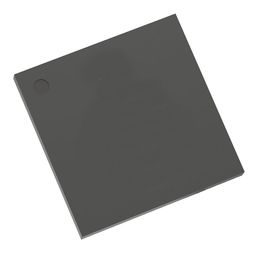
SLC NAND Flash Parallel 3.3V 4Gbit 512M x 8bit 25ns 63-Pin VFBGA Tray
替代料號:
MT29F4G08ABADAH4-IT:D
RoHS 6 Compliant
NAND Flash technology provides a cost-effective solution for applications requiring high-density, solid-state storage. The MT29F4G08AAA is a 4Gb NAND Flash memory device. The MT29F8G08BAA is a two-die stack that operates as a single 8Gb device. The MT29F8G08DAA is a two-die stack that operates as two independent 4Gb devices. The MT29F16G08FAA is a four-die stack that operates as two independent 8Gb devices, providing a total storage capacity of 16Gb in a single, space-saving package. Micron NAND Flash devices include standard NAND Flash features as well as new features designed to enhance system-level performance. Micron NAND Flash devices use a highly multiplexed 8-bit bus (I/O[7:0]) to transfer data, addresses, and instructions. The five command pins (CLE, ALE, CE#, RE#, WE#) implement the NAND Flash command bus interface protocol. Additional pins control hardware write protection (WP#) and monitor device status (R/B#). This hardware interface creates a low-pin-count device with a standard pinout that is the same from one density to another, allowing future upgrades to higher densities without board redesign. The MT29F4G, MT29F8G, and MT29F16G devices contain two planes per die. Each plane consists of 2,048 blocks. Each block is subdivided into 64 programmable pages. Each page consists of 2,112 bytes. The pages are further divided into a 2,048-byte data storage region with a separate 64-byte area. The 64-byte area is typically used for error management functions. The contents of each page can be programmed in 220µs (TYP), and an entire block can be erased in 1.5ms (TYP). On-chip control logic automates PROGRAM and ERASE operations to maximize cycle endurance. PROGRAM/ERASE endurance is specified at 100,000 cycles with appropriate error correction code (ECC) and error management.
技術參數
- Single-level cell (SLC) technology
- Organization
- Page size x8: 2,112 bytes (2,048 + 64 bytes)
- Block size: 64 pages (128K + 4K bytes)
- Plane size: 2,048 blocks
- Device size: 4Gb: 4,096 blocks; 8Gb: 8,192 blocks; 16Gb: 16,384 blocks
- READ performance
- Random READ: 25µs (MAX)
- Sequential READ: 25ns (MIN)
- WRITE performance
- PROGRAM PAGE: 220µs (TYP)
- BLOCK ERASE: 1.5ms (TYP)
- Data retention: 10 years
- Endurance: 100,000 PROGRAM/ERASE cycles
- First block (block address 00h) guaranteed to be valid up to 1,000 PROGRAM/ERASE cycles1
- Industry-standard basic NAND Flash command set
- Advanced command set:
- PROGRAM PAGE CACHE MODE
- PAGE READ CACHE MODE
- One-time programmable (OTP) commands
- Two-plane commands
- Interleaved die operations
- READ UNIQUE ID (contact factory)
- READ ID2 (contact factory)
- Operation status byte provides a software method of detecting:
- Operation completion
- Pass/fail condition
- Write-protect status
- Ready/busy# (R/B#) signal provides a hardware method of detecting operation completion
- WP# signal: write protect entire device
- RESET required after power-up
- INTERNAL DATA MOVE operations supported within the plane from which data is read
技術屬性
查找類似的料號|
|
描述 | 值 |
|---|---|---|
|
|
集成電路貼裝 | Surface Mount |
|
|
安裝 | Surface Mount |
|
|
鉛完成 | Tin-Silver-Copper |
|
|
Block Organization | Symmetrical |
|
|
Boot Block | No |
|
|
Maximum Operating Current | 35 mA |
|
|
引腳數 | 63 |
|
|
引腳數 | 63 |
|
|
Number of Words | 512 MWords |
|
|
最高加工溫度 | 260 |
|
|
最低工作溫度 | -40 °C |
|
|
工作溫度 | -40 to 85 °C |
|
|
接口 | Parallel |
|
|
最大電源電壓 | 3.6 V |
|
|
集成電路外殼/封裝 | VFBGA |
|
|
篩選級別 | Industrial |
|
|
Typical Operating Supply Voltage | 3.3000 V |
|
|
Program Current | 35 mA |
|
|
Simultaneous Read/Write Support | No |
|
|
ECC Support | Yes |
|
|
Density | 4 Gbit |
|
|
Maximum Erase Time | 0.003/Block s |
|
|
Maximum Programming Time | 0.6/Page ms |
|
|
產品尺寸 | 11 x 9 x 0.65 mm |
|
|
Address Bus Width | 1 Bit |
|
|
Architecture | Sectored |
|
|
Maximum Random Access Time | 25 ns |
|
|
接口類型 | Parallel |
|
|
Cell Type | SLC NAND |
|
|
Erase Suspend/Resume Modes Support | No |
|
|
Number of Bits per Word | 8 Bit |
|
|
閃存類型 | SLC NAND |
|
|
存儲密度 | 4 Gbit |
|
|
存取時間 | 25 ns |
|
|
最小電源電壓 | 2.7 V |
|
|
額定電源電壓 | 3.3 V |
|
|
最高工作溫度 | 85 °C |
|
|
供應商套餐 | VFBGA |
ECCN/UNSPSC
| 描述 | 值 |
|---|---|
| ECCN: | 3A991.a.1 |
| 計劃交貨期 B: | PARTS... |
| HTSN: | PARTS... |
文件
您需要登錄才能查看內容
文檔
| 標題 | 下載 | 類別 | 發布日期 |
|---|---|---|---|
| MIC4-MIC_31901 PCN | EOL-Documentation | 20160109 | |
| MIC4-MIC_31901 PCN | Other-Documents | 20160109 | |
| MIC4-PCN_31901 PCN | EOL-Documentation | 20160109 |


