製造商:
ISSI
IS42S16320D-6TL
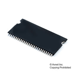
DRAM Chip SDRAM 512M-Bit 32Mx16 3.3V 54-Pin TSOP-II
替代料號:
IS42S16320D-6TL
RoHS 6 Compliant
NCNR
Obsolete
The 512Mb SDRAM is a high speed CMOS, dynamic random-access memory designed to operate in either 3.3V VDD/VDDQ or 2.5V VDD/VDDQ memory systems, depending on the DRAM option. Internally configured as a quad-bank DRAM with a synchronous interface. The 512Mb SDRAM (536,870,912 bits) includes an AUTO REFRESH MODE, and a power-saving, power-down mode. All signals are registered on the positive edge of the clock signal, CLK. All inputs and outputs are LVTTL compatible. The 512Mb SDRAM has the ability to synchronously burst data at a high data rate with automatic column-address generation, the ability to interleave between internal banks to hide precharge time and the capability to randomly change column addresses on each clock cycle during burst access. A self-timed row precharge initiated at the end of the burst sequence is available with the AUTOPRECHARGE function enabled. Precharge one bank while accessing one of the other three banks will hide the precharge cycles and provide seamless, high-speed, random-access operation. SDRAM read and write accesses are burst oriented starting at a selected location and continuing for a programmed number of locations in a programmed sequence. The registration of an ACTIVE command begins accesses, followed by a READ or WRITE command. The ACTIVE command in conjunction with address bits registered are used to select the bank and row to be accessed (BA0, BA1 select the bank; A0-A12 select the row). The READ or WRITE commands in conjunction with address bits registered are used to select the starting column location for the burst access. Programmable READ or WRITE burst lengths consist of 1, 2, 4 and 8 locations or full page, with a burst terminate option.
技術參數
- Clock frequency: 200, 166, 143 MHz
- Fully synchronous; all signals referenced to a positive clock edge
- Internal bank for hiding row access/precharge
- Power supply: IS42S16320D - VDD/VDDQ = 3.3V
- LVTTL interface
- Programmable burst length
- 1, 2, 4, 8, full page
- Programmable burst sequence: Sequential/Interleave
- Auto Refresh (CBR)
- Self Refresh
- 8K refresh cycles every 64 ms
- Random column address every clock cycle
- Programmable CAS latency (2, 3 clocks)
- Burst read/write and burst read/single write operations capability
- Burst termination by burst stop and precharge command
- Packages:
- x8/x16: 54-pin TSOP-II, 54-ball TF-BGA (x16 only)
- x32: 90-ball TF-BGA
- Temperature Range:
- Commercial (0°C to +70°C)
- Industrial (-40°C to +85°C)
- Automotive, A1 (-40°C to +85°C)
- Automotive, A2 (-40°C to +105°C)
技術屬性
查找類似的料號|
|
描述 | 值 |
|---|---|---|
|
|
安裝 | Surface Mount |
|
|
最高加工溫度 | 260 |
|
|
工作溫度 | 0 to 70 °C |
|
|
引腳數 | 54 |
|
|
供應商套餐 | TSOP-II |
|
|
集成電路貼裝 | Surface Mount |
|
|
工作電源電壓 | 2.7, 5.5 V |
|
|
Maximum Random Access Time | 6|5.4 ns |
|
|
最低工作溫度 | 0 °C |
|
|
數據總線寬度 | 16 Bit |
|
|
Maximum Clock Rate | 167 MHz |
|
|
鉛完成 | Matte Tin |
|
|
Density | 512 Mbit |
|
|
Address Bus Width | 15 Bit |
|
|
Number of I/O Lines | 16 Bit |
|
|
篩選級別 | Commercial |
|
|
Maximum Operating Current | 180 mA |
|
|
產品尺寸 | 22.42 x 10.29 x 1.05 mm |
|
|
最高工作溫度 | 70 °C |
|
|
Number of Bits per Word | 16 Bit |
|
|
額定電源電壓 | 3.3 V |
|
|
存儲密度 | 512 Mbit |
|
|
時鐘頻率最大值 | 167 MHz |
|
|
集成電路外殼/封裝 | TSOP-II |
|
|
MSL 級別 | MSL 3 - 168 hours |
|
|
引腳數 | 54 |
|
|
類型 | SDRAM |
ECCN/UNSPSC
| 描述 | 值 |
|---|---|
| ECCN: | EAR99 |
| 計劃交貨期 B: | 8542320015 |
| HTSN: | 8542320028 |

