
NB3F8L3005CMNTBG


Technical Attributes
Find Similar Parts
| Description | Value | |
|---|---|---|
| Fanout Buffer | ||
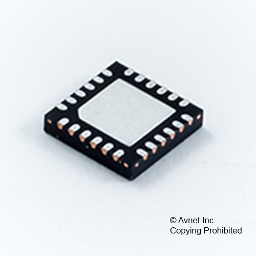
| QFN-EP | ||
| 50 MHz | ||
| 10 MHz | ||
| HCSL, LVCMOS, LVDS, LVPECL, LVTTL, SSTL | ||
| 1 | ||
| 5 | ||
| 24 | ||
| 85 °C | ||
| -40 °C | ||
| LVCMOS, LVTTL | ||
| NB3F8L3005C Series | ||
| 3.465 Vdc | ||
| 3.135 Vdc |
ECCN / UNSPSC / COO
| Description | Value |
|---|---|
| Country of Origin: | null |
| ECCN: | EAR99 |
| HTSN: | 8542390001 |
| Schedule B: | 8542390000 |