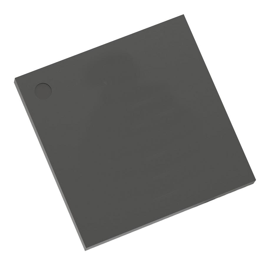
MT41K512M16VRP-107 AAT:P
DRAM Chip DDR3L SDRAM 8Gbit 512M x 16 1.35V 96-Pin FPBGA T/R
MT41K512M16VRP-107 AAT:P is a TwinDie 1.35V DDR3L SDRAM. It is a high-speed, CMOS dynamic random access memory device internally configured as two 8-bank DDR3L SDRAM. It uses a double data rate architecture to achieve high-speed operation. The double data rate architecture is an 8n-prefetch architecture with an interface designed to transfer two data words per clock cycle at the I/O balls. A single read or write access consists of a single 8n-bit-wide, one-clock-cycle data transfer at the internal DRAM core and eight corresponding n-bit-wide, one-half-clock-cycle data transfers at the I/O balls.
- 512Meg x 16 configuration, data rate is 1866MT/s, automotive certified
- Packaging style is 96-ball FBGA, 8mm x 14mm
- Timing (cycle time) is 1.07ns at CL = 13 (DDR3-1866)
- Operating temperature range is –40°C to +105°C, automotive certification
- Supply voltage range is –0.4V to 1.975V, output driver calibration
- Differential bidirectional data strobe, 8n-bit prefetch architecture
- Differential clock inputs (CK, CK#), 8 internal banks, multipurpose register
- Programmable CAS (READ) latency (CL), programmable CAS (WRITE) latency (CWL)
- Selectable BC4 or BL8 on-the-fly (OTF), self refresh mode
- Self refresh temperature (SRT), automatic self refresh (ASR)
Technical Attributes
Find Similar Parts
| Description | Value | |
|---|---|---|
| 14 Bit | ||
| 933 MHz | ||
| 16 Bit | ||
| 8 Gbit | ||
| DDR3L SDRAM | ||
| TFBGA | ||
| Surface Mount | ||
| Tin-Silver-Copper | ||
| 260 °C | ||
| 933 MHz | ||
| 88 mA | ||
| 1.07 ns | ||
| 512M x 16bit | ||
| 8 Gbit | ||
| Surface Mount | ||
| 96 | ||
| 8 | ||
| 16 Bit | ||
| 16 Bit | ||
| 3, 5 V | ||
| -40 to 105 °C | ||
| 105 °C | ||
| -40 °C | ||
| 512M x 16 | ||
| 96FBGA | ||
| 96 | ||
| 8 x 14 x 0.72 mm | ||
| Automotive | ||
| FPBGA | ||
| 1.35 V | ||
| DDR3L SDRAM |
ECCN / UNSPSC / COO
| Description | Value |
|---|---|
| Country of Origin: | null |
| ECCN: | EAR99 |
| HTSN: | 8542320032 |
| Schedule B: | null |

