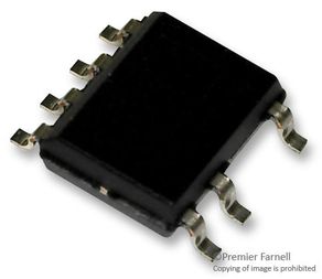
制造商:
Power Integrations
LNK605DG-TL
LED Driver AC/DC, CV/CC Switcher, Flyback, 90V to 265V Input, 65W, 80kHz, 1 Output, SOIC-8
安富利制造商模型#:
LNK605DG-TL
RoHS 6 Compliant
LinkSwitch™-II dramatically simplifies low power CV/CC charger designs by eliminating an optocoupler and secondary control circuitry. The device introduces a revolutionary control technique to provide very tight output voltage and current regulation, compensating for transformer and internal parameter tolerances along with input voltage variations. The device incorporates a 700V power MOSFET, a novel ON/OFF control state machine, a high-voltage switched current source for self-biasing, frequency jittering, cycle-by-cycle current limit and hysteretic thermal shutdown circuitry onto a monolithic IC. It compensates for transformer inductance tolerances, input line voltage variations and external component temperature variations. Auto-restart protection reduces power delivered by 95% for output short-circuit and control loop faults (open and shorted components). Applications includes chargers for cell/cordless phones, PDAs, MP3/portable audio devices, adapters and LED drivers.
技术参数
- Output power of 4.5W (adapter), 5.1W (open frame) at 85-265VAC
- Energy efficient, accurate CV/CC switcher for adapters and chargers
- Dramatically simplifies CV/CC converters, EcoSmartâ„¢ energy efficient
- Eliminates optocoupler, all secondary CV/CC control and all control loop compensation circuitry
- Very tight IC parameter tolerances using proprietary trimming technology
- Frequency jittering greatly reduces EMI filter cost, meets all global energy efficiency regulations
- Meets high-voltage creepage requirements between DRAIN and all other pins both on PCB and at package
- No-load consumption below 30mW at 230VAC with optional external bias winding
- ON/OFF control provides constant efficiency down to very light loads
- No current sense resistors, maximizes efficiency, hysteretic thermal shutdown
技术特性
查找类似的料号|
|
描述 | 值 |
|---|---|---|
|
|
最低工作温度 | -40 °C |
|
|
集成电路外壳/封装 | SOIC |
|
|
拓扑结构 | Flyback |
|
|
最高工作温度 | 150 °C |
|
|
输出个数 | 1 |
|
|
集成电路安装 | Surface Mount |
|
|
输入电压最小值 | 85 V |
|
|
输入电压最大值 | 265 V |
|
|
引脚数 | 8 |
|
|
产品范围 | LinkSwitch-II Series |
|
|
输出电流最大值 | 337 mA |
|
|
典型开关频率 | 85 kHz |
|
|
输出电压最大值 | 12.1 V |
ECCN / UNSPSC
| 描述 | 值 |
|---|---|
| ECCN: | EAR99 |
| 计划交货期 B: | PARTS... |
| HTSN: | PARTS... |


