Manufacturer:
onsemi
FOD3184
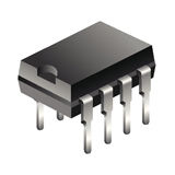
Optocoupler DC-IN 1-CH Transistor With Base DC-OUT 8-PIN DIP Tube
Avnet Manufacturer Part #:
FOD3184
RoHS 10 Compliant
The FOD is an advanced 2.5 A output current IGBT drive optocoupler capable of driving most 1200 V / 150 A IGBTs. It is ideally suited for fast-switching driving of power IGBTs and MOSFETs used in motor-control inverter applications and high-performance power systems. The FOD8316 offers critical protection features necessary for preventing fault conditions that lead to destructive thermal runaway of IGBTs. The device utilizes Fairchild's proprietary Opt planar coplanar packaging technology, and optimized IC design to achieve high noise immunity, characterized by high common-mode rejection and power supply rejection specifications. The FOD8316 consists of an integrated gate drive optocoupler featuring low RDs(0N) CMOS transistors to drive the IGBT from rail-to-rail and an integrated high-speed isolated feedback for fault sensing. The device is housed in a compact 16-pin small-outline plastic package which meets the 8 mm creep age and clearance requirements.
Key Features
- High Noise Immunity Characterized by Common Mode Rejection - 35 kV/μs Minimum, VCM = 1500 Vpeak
- 2.5 A Peak Output Current Driving Capability for Most 1200 V / 150 A IGBTs
- Optically Isolated Fault Sensing Feedback
- soft" IGBT Turn-off
- Built-in IGBT protection
- Desaturation Detection
- Under-voltage Lockout (UVLO) Protection
- Wide Supply Voltage Range: 15 V to 30 V
- P-channel MOSFETS at output stage Enables Output Voltage Swing Close to the Supply Rail (Rail-to-Rate output)
- 3.3 V/ 5 V, CMOS/TTL compatible Inputs
- High Speed
- 500 ns Maximum Propagation Delay Over Full Operating Temperature Range
- Extended Industrial Temperate Range: -40 °C to 100°C
- Safety and Regulatory Approvals
- ULIS77, 4,243 tor 1 Minute
- DIN EN,'IEC 60747-5-5 1 ,414 VPEAK Working Insulation Voltage Rating 8,000 VPEAK Transient Isolation Voltage Rating
- RDS(ON) at 1Ω (Typical) Offers Lower Power Dissipation
- User-configurable: Inverting, Non-inverting, Auto-reset, Auto-shutdown
- 8 mm Creep age and Clearance Distances
Technical Attributes
Find Similar Parts|
|
Description | Value |
|---|---|---|
|
|
Product Dimensions | 9.91 x 6.86 x 3.94 mm |
|
|
Lead Finish | Tin |
|
|
Supplier Package | DIP |
|
|
Maximum Power Dissipation | 295 mW |
|
|
Pin Count | 8 |
|
|
Peak Forward Voltage | 1.8 V |
|
|
Operating Temperature | -40 to 100 °C |
|
|
Output Device | MOSFET |
|
|
Input Type | DC |
|
|
Max Processing Temp | 260 °C |
|
|
Output Type | DC |
|
|
Maximum Fall Time | 24 ns |
|
|
Mounting | Through Hole |
|
|
Number of Channels per Chip | 1 |
|
|
Maximum Rise Time | 38 ns |
|
|
Reverse Voltage | 5 V |
|
|
Input Current | 25 mA |
|
|
Minimum Isolation Voltage | 5000 Vrms |
|
|
Screening Level | Extended Industrial |
ECCN / UNSPSC / COO
| Description | Value |
|---|---|
| ECCN: | EAR99 |
| SCHEDULE B: | 8541408000 |
| HTSN: | 8541408000 |


