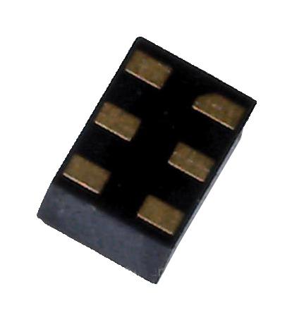
Manufacturer:
Nexperia
74AUP1G373GM,115
Latch, 74AUP1G373, D Type Transparent, Tri State, 6.4 ns, 4 mA, 6 Pins, XSON
Avnet Manufacturer Part #:
74AUP1G373GM,115
RoHS 6 Compliant
The 74AUP1G373 provides the single D-type transparent latch with 3-state output. While the latch-enable (LE) input is high, the Q output follows the data (D) input. When pin LE is LOW, the latch stores the information that was present at the D-input one set-up time preceding the HIGH-to-LOW transition of pin LE. When pin OE is LOW, the contents of the latch is available at the (Q) output. When pin OE is HIGH, the output goes to the high-impedance OFF-state. Operation of input pin OE does not affect the state of the latch. Schmitt trigger action at all inputs makes the circuit tolerant to slower input rise and fall times across the entire Vcc range from 0.8 V to 3.6 V. This device ensures a very low static and dynamic power consumption across the entire Vcc range from 0.8 V to 3.6 V. This device is fully specified for partial power-down applications using Ioff. The Ioff circuitry disables the output, preventing the damaging backflow current through the device when it is powered down.
Key Features
- Wide supply voltage range from 0.8 V to 3.6 V
- High noise immunity
- Complies with JEDEC standards:
- JESD8-12 (0.8 V to 1.3 V)
- JESD8-11 (0.9 V to 1.65 V)
- JESD8-7 (1.2 V to 1.95 V)
- JESD8-5 (1.8 V to 2.7 V)
- JESD8-B (2.7 V to 3.6 V)
- ESD protection:
- HBM JESD22-A114F Class 3A exceeds 5000 V
- MM JESD22-A115-A exceeds 200 V
- CDM JESD22-C101E exceeds 1000 V
- Low static power consumption; Icc = 0.9 µA (maximum)
- Latch-up performance exceeds 100 mA per JESD 78 Class II
- Inputs accept voltages up to 3.6 V
- Low noise overshoot and undershoot < 10 % of Vcc
- Ioff circuitry provides partial Power-down mode operation
- Multiple package options
- Specified from -40 °C to +85 °C and -40 °C to +125 °C
Technical Attributes
Find Similar Parts|
|
Description | Value |
|---|---|---|
|
|
Operating Temperature Max | 125 °C |
|
|
No. of Pins | 6 |
|
|
Operating Temperature Min | -40 °C |
|
|
Supply Voltage Max | 3.6 V |
|
|
Output Current | 4 mA |
|
|
No. of Channels | 1 |
|
|
Supply Voltage Min | 800 mV |
|
|
No. of Elements | One |
|
|
Propagation Delay | 6.4 ns |
|
|
IC Output Type | Tri State |
|
|
Latch Type | D Type Transparent |
|
|
Logic IC Family | 74AUP |
|
|
No. of Bits | 1bit |
|
|
Logic Family / Base Number | 74AUP1G373 |
|
|
Logic IC Base Number | 741G373 |
|
|
IC Case / Package | XSON |
ECCN / UNSPSC / COO
| Description | Value |
|---|---|
| ECCN: | EAR99 |
| SCHEDULE B: | 8542390000 |
| HTSN: | 8542390001 |
Documents
Please log in to view more information.
Documents
| Title | Download | Type | Date Published |
|---|---|---|---|
| Improved BOM of leadless 5/6 pad packages, including die optimization to achieve zero delamination in ATSN (Nexperia Assembly & Test Plant Seremban Malaysia) | PCN-Documentation | 20191231 |
