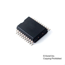
TC74VHC273F(ELKF
Flip Flop D-Type Bus Pos-Edge 8-Element 20-Pin SOP
The TC74VHC273 is an advanced high speed CMOS OCTAL D-TYPE FLIP FLOP fabricated with silicon gate C2MOS technology.
It achieves the high speed operation similar to equivalent Bipolar Schottky TTL while maintaining the CMOS low power dissipation.
Information signals applied to D inputs are transferred to the Q outputs on the positive going edge of the clock pulse. When the CLR input is held “L”, the Q outputs are at a low logic level independent of the other inputs.
An input protection circuit ensures that 0 to 5.5 V can be applied to the input pins without regard to the supply voltage. This device can be used to interface 5 V to 3 V systems and two supply systems such as battery back up. This circuit prevents device destruction due to mismatched supply and input voltages.
Key Features
- High speed: fmax = 165 MHz (typ.) at VCC = 5 V
- Low power dissipation: ICC = 4 μA (max) at Ta = 25°C
- High noise immunity: VNIH = VNIL = 28% VCC (min)
- Power down protection is provided on all inputs.
- Balanced propagation delays: tpLH ∼− tpHL
- Wide operating voltage range: VCC (opr) = 2 to 5.5 V
- Low noise: VOLP = 0.8 V (max)
- Pin and function compatible with 74ALS273
Technical Attributes
Find Similar Parts|
|
Description | Value |
|---|---|---|
|
|
Number of Element Inputs | 8 |
|
|
IC Case / Package | SOP |
|
|
Number of Channels per Chip | 8 |
|
|
Maximum Low Level Output Current | 8 mA |
|
|
Number of Element Outputs | 8 |
|
|
Triggering Type | Positive-Edge |
|
|
Maximum Operating Supply Voltage | 5.5 V |
|
|
Minimum Operating Supply Voltage | 2 V |
|
|
Set/Reset | Master Reset |
|
|
Input Signal Type | Single-Ended |
|
|
Output Signal Type | Single-Ended |
|
|
Bus Hold | No |
|
|
Number of Elements per Chip | 1 |
|
|
Flip-Flop Type | D |
|
|
Propagation Delay | 17.1 ns |
|
|
IC Output Type | Non-Inverting |
|
|
Typical Operating Supply Voltage | 2.5|3.3|5 V |
|
|
No. of Pins | 20 |
ECCN / UNSPSC / COO
| Description | Value |
|---|---|
| ECCN: | EAR99 |
| SCHEDULE B: | PARTS... |
| HTSN: | PARTS... |
