Manufacturer:
Nordic Semiconductor
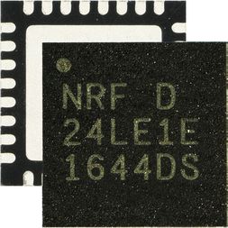
NRF24LE1-O17Q32-R
Ultra Low Power Wireless SoC, ESB, 32 Pins, QFN-EP
Avnet Manufacturer Part #:
NRF24LE1-O17Q32-R
RoHS 10 Compliant
The nRF24LE1 is a member of the low-cost, high-performance family of intelligent 2.4 GHz RF transceivers with embedded microcontrollers. The nRF24LE1 is optimized to provide a single chip solution for ULP wireless applications. The combination of processing power, memory, low power oscillators, real-time counter, AES encryption accelerator, random generator and a range of power saving modes provides an ideal platform for implementation of RF protocols. Benefits of using nRF24LE1 include tighter protocol timing, security, lower power consumption and improved co-existence performance. For the application layer the nRF24LE1 offers a rich set of peripherals including: SPI, 2-wire, UART, 6 to 12 bit ADC, PWM and an ultra low power analog comparator for voltage level system wake-up. The nRF24LE1 comes in three different package variants: • An ultra compact 4×4mm 24 pin QFN (7 generic I/O pins) • A compact 5×5mm 32 pin QFN (15 generic I/O pins) • A 7×7mm 48 pin QFN (31 generic I/O pins) The 4×4mm 24 pin QFN is ideal for low I/O count applications where small size is key. Examples include wearable sports sensors and watches. The 5×5mm 32 pin QFN is ideal for medium I/O count applications such as wireless mouse, remote controls and toys. The 7×7mm 48 pin QFN is designed for high I/O count products like wireless keyboards.
Key Features
- Fast 8-bit microcontroller:
- Intel MCS 51 compliant instruction set
- Reduced instruction cycle time, up to 12 times compared to legacy 8051
- 32 bit multiplication - division unit
- Memory:
- Program memory: 16 kB of Flash memory with security features (up to 1k erase/ write cycles)
- Data memory: 1 kB of on-chip RAM memory
- Non-volatile data memory: 1 kB
- Non-volatile data memory extended endurance: 512 bytes (up to 20k erase/ write cycles)
- A number of on-chip hardware resources are available through programmable multi-purpose input/output pins (7-31 pins dependent on package variant):
- GPIO
- SPI master
- SPI slave
- 2-Wire master/ slave
- Full duplex serial port
- PWM
- ADC
- Analog comparator
- External interrupts
- Timer inputs
- 32.768 kHz crystal oscillator
- Debug interface
- High performance 2.4 GHz RF-transceiver
- True single chip GFSK transceiver
- Enhanced ShockBurst™ link layer support in HW:
- Packet assembly/disassembly
- Address and CRC computation
- Auto ACK and retransmit
- On the air data rate 250 kbps, 1 Mbps or 2 Mbps
- Digital interface (SPI) speed 0-8 Mbps
- 125 RF channel option, with 79 (2.402 GHz-2.480 GHz) channels within 2.400 - 2.4835 GHz
- Short switching time enable frequency hopping
- Fully RF compatible with nRF24LXX
- RF compatible with nRF24E1 in 250 kbps and 1 Mbps mode
- A/D converter:
- 6, 8, 10 or 12 bit resolution
- 14 input channels
- Single ended or differential input
- Full-scale range set by internal reference, external reference or VDD
- Single step mode with conversion time down to 3 µs
- Continuous mode with 2, 4, 8 or 16 kbps sampling rate
- Low current consumption; only 0.1mA at 2 ksps
- Mode for measuring supply voltage
Technical Attributes
Find Similar Parts|
|
Description | Value |
|---|---|---|
|
|
IC Case / Package | QFN-EP |
|
|
No. of Pins | 32 |
|
|
Frequency Response RF Max | 2525 MHz |
|
|
Operating Temperature Range | -40°C to 85°C |
|
|
Interfaces | I2C, PWM, SPI, UART |
|
|
Protocol | ESB |
|
|
Supply Voltage Range | 1.9V to 3.6V |
|
|
SoC Type | Ultra Low Power Wireless SoC |
ECCN / UNSPSC / COO
| Description | Value |
|---|---|
| ECCN: | EAR99 |
| SCHEDULE B: | PARTS... |
| HTSN: | PARTS... |

