Manufacturer:
Nexperia
74LVC573ABQ,115
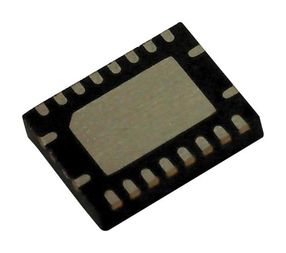
Latch, 74LVC573, D Type Transparent, Tri State, 8 ns, 24 mA, 20 Pins, DHVQFN
Avnet Manufacturer Part #:
74LVC573ABQ,115
RoHS 6 Compliant
The 74LVC573A consists of eight D-type transparent latches, featuring separate D-type inputs for each latch and 3-state true outputs for bus-oriented applications. A Latch Enable (LE) input and an Output Enable input are common to all internal latches. When LE is HIGH, data at the Dn inputs enters the latches. In this condition, the latches are transparent, that is, a latch output changes each time its corresponding D-input changes. When LE is LOW, the latches store the information that was present at the D-inputs one set-up time preceding the HIGH-to-LOW transition of LE. When Output Enable is LOW, the contents of the eight latches are available at the outputs. When Output Enable is HIGH, the outputs go to the high impedance OFF-state. Operation of the Output Enable input does not affect the state of the latches. Inputs can be driven from either 3.3 V or 5 V devices. When disabled, up to 5.5 V can be applied to the outputs. These features allow the use of these devices as translators in mixed 3.3 V or 5 V applications. The 74LVC573A is functionally identical to the 74LVC373A, but has a different pin arrangement.
Key Features
- 5 V tolerant inputs/outputs, for interfacing with 5 V logic
- Supply voltage range from 1.2 V to 3.6 V
- CMOS low power consumption
- Direct interface with TTL levels
- High-impedance when VCC = 0 V
- Flow-through pinout architecture
- Complies with JEDEC standard:
- JESD8-7A (1.65 V to 1.95 V)
- JESD8-5A (2.3 V to 2.7 V)
- JESD8-C/JESD36 (2.7 V to 3.6 V)
- ESD protection:
- HBM JESD22-A114F exceeds 2000 V
- MM JESD22-A115-B exceeds 200 V
- CDM JESD22-C101E exceeds 1000 V
- Specified from -40 °C to +85 °C and -40 °C to +125 °C
Technical Attributes
Find Similar Parts|
|
Description | Value |
|---|---|---|
|
|
Operating Temperature Max | 125 °C |
|
|
IC Case / Package | DHVQFN |
|
|
No. of Bits | 8bit |
|
|
Supply Voltage Max | 3.6 V |
|
|
Operating Temperature Min | -40 °C |
|
|
Supply Voltage Min | 1.2 V |
|
|
No. of Channels | 8 |
|
|
No. of Elements | One |
|
|
Propagation Delay | 8 ns |
|
|
IC Output Type | Tri State |
|
|
Output Current | 24 mA |
|
|
Logic Family / Base Number | 74LVC573 |
|
|
Latch Type | D Type Transparent |
|
|
Logic IC Base Number | 74573 |
|
|
Logic IC Family | 74LVC |
|
|
No. of Pins | 20 |
ECCN / UNSPSC / COO
| Description | Value |
|---|---|
| ECCN: | EAR99 |
| SCHEDULE B: | 8542390000 |
| HTSN: | 8542390001 |

