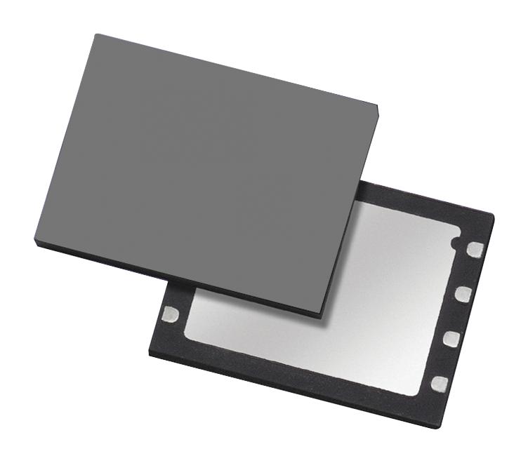
IS25LP064A-JKLE
NOR Flash Serial-SPI 3V 64Mbit 64M 1bit 8ns 8-Pin WSON
The IS25LP064A Serial Flash memory offers a versatile storage solution with high flexibility and performance in a simplified pin count package. Flash are for systems that require limited space, a low pin count, and low power consumption. The device is accessed through a 4- wire SPI Interface consisting of a Serial Data Input (SI), Serial Data Output (SO), Serial Clock (SCK), and Chip Enable (CE#) pins, which can also be configured to serve as multi-I/O (see pin descriptions). The device supports Dual and Quad I/O as well as standard, Dual Output, and Quad Output SPI. Clock frequencies of up to 133MHz allow for equivalent clock rates of up to 532MHz (133MHz x 4) which equates to 66Mbytes/s of data throughput. The IS25xP series of Flash adds support for DTR (Double Transfer Rate) commands that transfer addresses and read data on both edges of the clock. These transfer rates can outperform 16-bit Parallel Flash memories allowing for efficient memory access to support XIP (execute in place) operation. The memory array is organized into programmable pages of 256-bytes. This family supports page program mode where 1 to 256 bytes of data are programmed in a single command. QPI (Quad Peripheral Interface) supports 2-cycle instruction further reducing instruction times. Pages can be erased in groups of 4Kbyte sectors, 32Kbyte blocks, 64Kbyte blocks, and/or the entire chip. The uniform sector and block architecture allows for a high degree of flexibility so that the device can be utilized for a broad variety of applications requiring solid data retention.
- Industry Standard Serial Interface
- IS25LP064A: 64Mbit/8Mbyte
- IS25LP032A: 32Mbit/4Mbyte
- 256 bytes per Programmable Page
- Supports standard SPI, Fast, Dual, Dual I/O, Quad, Quad I/O, SPI DTR, Dual I/O DTR, Quad I/O DTR, and QPI
- Double Transfer Rate (DTR) option
- Supports Serial Flash Discoverable Parameters (SFDP)
- High Performance Serial Flash (SPI)
- 133Mhz Fast Read at Vcc=2.7V to 3.6V
- 104Mhz Fast Read at Vcc=2.3V to 3.6V
- 532MHz equivalent at QPI operation
- 50MHz Normal Read
- DTR (Dual Transfer Rate) up to 66MHz
- Selectable dummy cycles
- Configurable drive strength
- Supports SPI Modes 0 and 3
- More than 100,000 erase/program cycles
- More than 20
- year data retention
- Flexible and Efficient Memory Architecture
- Chip Erase with Uniform Sector/block Erase (4/32/64 Kbyte)
- Program 1 to 256 bytes per page
- Pr
Technical Attributes
Find Similar Parts
| Description | Value | |
|---|---|---|
| 8 ns | ||
| 24 Bit | ||
| Sectored | ||
| Symmetrical | ||
| Yes | ||
| NOR | ||
| 133 MHz | ||
| 64 Mbit | ||
| No | ||
| Yes | ||
| Serial-SPI | ||
| 4-Wire, DTR, QPI, SPI | ||
| Bottom|Top | ||
| 260 | ||
| 45/Chip s | ||
| 13 mA | ||
| 1/Page ms | ||
| 8 ns | ||
| 64 Mbit | ||
| Surface Mount | ||
| MSL 3 - 168 hours | ||
| 8 | ||
| 1 Bit | ||
| 64 MWords | ||
| -40 to 105 °C | ||
| 105 °C | ||
| -40 °C | ||
| 8WSON | ||
| 8 | ||
| 6 x 5 x 0.8(Max) | ||
| 30 mA | ||
| 2.3 to 3.6 V | ||
| No | ||
| Extended Industrial | ||
| No | ||
| WSON | ||
| 3.6 V | ||
| 2.3 V | ||
| 3 V | ||
| 3.0000 V |
ECCN / UNSPSC / COO
| Description | Value |
|---|---|
| Country of Origin: | null |
| ECCN: | 3A991.b.1.a |
| HTSN: | PARTS... |
| Schedule B: | PARTS... |

