
Empowering the next generation of high-performance systems
All modern Silicon power devices are trench based and have replaced the planar technologies so what about Silicon Carbide? For SiC, there are many similarities with the Silicon power MOSFET technology evolution when it comes to performance advantages by trench design. One more striking advantage comes in addition with trench design in SiC, namely reliability. Vertical interfaces show significantly lower defect density compared to lateral ones in SiC material. This opens up a new optimization potential for matching performance and robustness features with reliability. Reliability is the fundament of every power device development at Infineon and CoolSiC™ MOSFET G2 trench technology maintains the high G1 reliability. DPM (defects per million) data based on all CoolSiC™ MOSFETs G1 sold, discretes and modules industrial grade, shows that product returns for SiC are even below silicon based power switches, a very mature technology. Infineon has also pioneered in application lifetime testing and certain tests are nowadays included in the JEDEC standard. The CoolSiC™ trench MOSFET design drives sustainable competitiveness for energy efficiency, now and in the future.
Explore how the new CoolSiC™ MOSFET Generation 2 trench MOSFET enables a new level of SiC performance, while meeting the highest quality standards in all common combinations of power schemes: AC-DC, DC-DC and DC-AC. Photovoltaic inverters, energy storage systems, EV charging, power supplies, motor drives and more belong to the many cases where SiC MOSFETs provide additional performance, compared to Si alternatives.
Learn about a series of new robustness features in CoolSiC™ MOSFET G2 products for reaching the best performance during long-term field operation.
Energy efficiency for every Watt of power processed
Power losses matter. Explore how the new CoolSiC™ MOSFET G2 trench technology improves on power delivery in common topologies used in AC/DC, DC/DC, DC/AC power schemes. Key figures-of-merit for both, hard-switching and soft-switching MOSFET operation, are improved by more than 20% compared to the previous generation. The fast switching capability, i.e. the signature of SiC MOSFETs, is in addition improved by more than 30%. As a result, G2 operates with lower power losses in all operation modes in photovoltaic inverters, energy storage installations, EV charging, UPS and more.
Raising the bar for the power possible in a given form factor
Combining the best of SiC: low power losses in small form factors. The lower is the on-resistance of a SiC MOSFET, the lower are the conduction losses, allowing more energy efficiency, power density and part count reduction. CoolSiC™ G2 MOSFET portfolios boost the lowest Rdson in the SiC MOSFET market. The introduction of best in class products in SMD packages, makes 7 mOhm rating in 650 V and 8 mOhm rating in 1200 V available in TO263-7 form factor. Improved package interconnect with .XT results in less thermal resistance, more output power, lower operating temperature.The power that can be delivered by an SMD form factor is increased by more than 60%, and raises the bar for power density possible in power conversion schemes.
Setting a new standard for utilization of SiC performance
Ideally suited for hard- and
resonant-switching topologies
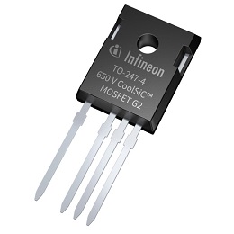
Our range of 650 V CoolSiC™ MOSFETs offer optimized switching behaviors at high currents and low capacitances and are designed for a variety of industrial applications including, servers, telecom, motor drives, and more.
Reaching the best performance
during long-term field operation.
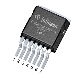
The 1200 V MOSFET range is available for both industrial and automotive qualified applications, such as on-board charger/PFC, auxiliary inverters, and uninterruptible power supply (UPS). With the example of three-phase power schemes, compared to the previous generation 1200 V CoolSiC™ G2 operates at 5-30% lower power losses depending on the load condition, enabling energy savings for every Watt processed in the field.
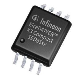
Designed for MOSFETs, IGBTs, SiC MOSFETs and GaN HEMTs
EiceDRIVER™ gate drivers provide a wide range of typical output current options, from 0.1-A up to 10-A. Robust gate drive protection features such as fast short-circuit protection (DESAT), active Miller clamp, shoot-through protection, fault, shutdown, and over current protection, make these driver ICs well-suited for both silicon and wide-bandgap power devices, including CoolGaN™, and CoolSiC™.