
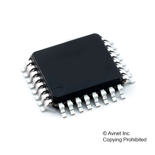
MC100EP195BFAG
3.3 V ECL Programmable Delay Chip
-
 RoHS 10 Compliant
 -
 Tariff Charges
The MC100EP195B is a Programmable Delay Chip (PDC) designed primarily for clock deskewing and timing adjustment. It provides variable delay of a differential NECL/PECL input transition. Thedelay section consists of a programmable matrix of gates and multiplexers. The delay increment of the EP195B has a digitally selectable resolution of about 10 ps and a net range of up to 10.2 ns. The required delay is selected by the 10 data select inputs D(9:0) values and controlled by the LEN (pin 10). A LOW level on LEN allows a transparent LOAD mode of real time delay values by D(9:0). A LOW to HIGH transition on LEN will LOCK and HOLD currentvalues present against any subsequent changes in D(10:0). The approximate delay values for varying tap numbers correlating to D0 (LSB) through D9 (MSB).
- Maximum Input Clock Frequency >1.2 GHz Typical
- Programmable Range: 0 ns to 10 ns
- Delay Range: 2.2 ns to 12.2 ns
- 10 ps Increments
- PECL Mode Operating Range:VCC = 3.0 V to 3.6 V with VEE = 0 V
- NECL Mode Operating Range:VCC = 0 V with VEE = 3.0 V to 3.6 V
- IN/INb Inputs Accept LVPECL, LVNECL, LVDS Levels
- A Logic High on the EN Pin Will Force Q to Logic Low
- D10:0 Can Select Either LVPECL, LVCMOS, or LVTTL Input Levels
- VBB Output Reference Voltage
Technical Attributes
Find Similar Parts
| Description | Value | |
|---|---|---|
| Programmable Delay Line | ||
| LQFP | ||
| 32 | ||
| 1024 | ||
| 0.01 ns | ||
| 85 °C | ||
| -40 °C | ||
| MC100EP195B Series | ||
| 3.6 Vdc | ||
| 3 Vdc | ||
| 12.2 ns |
ECCN / UNSPSC / COO
| Description | Value |
|---|---|
| Country of Origin: | null |
| ECCN: | EAR99 |
| HTSN: | 8542390001 |
| Schedule B: | 8542390000 |