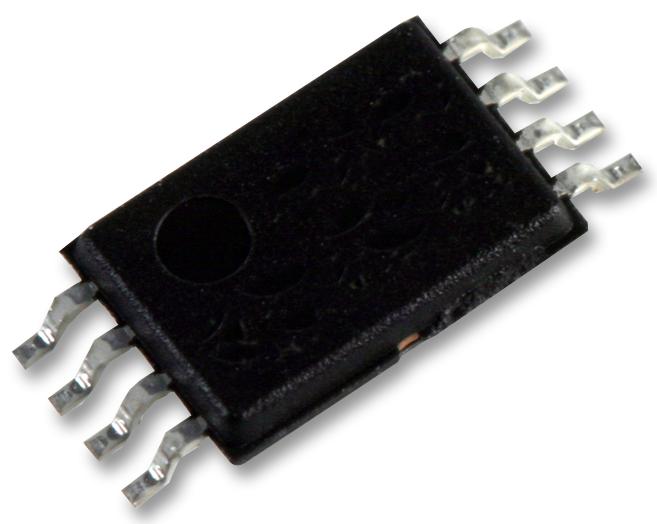
74LVC1G79GW,125
Flip Flop, 74LVC1G79, D, 5 ns, 500 MHz, 32 mA, 5 Pins, TSSOP
- RoHS 10 Compliant
- Tariff Charges
The 74LVC1G79GW is a single positive-edge triggered D-type Flip-flop features that the information on the data input is transferred to the Q-output on the low-to-high transition of the clock pulse. The D-input must be stable one set-up time prior to the low-to-high clock transition for predictable operation. Inputs can be driven from either 3.3 or 5V devices. This feature allows the use of this device in a mixed 3.3 and 5V environment. This device is fully specified for partial power-down applications using IOFF. The IOFF circuitry disables the output, preventing the damaging backflow current through the device when it is powered down.
- High noise immunity
- CMOS low power consumption
- Latch-up performance exceeds 250mA
- Direct interface with TTL levels
- ±24mA Output drive current
Technical Attributes
Find Similar Parts
| Description | Value | |
|---|---|---|
| No | ||
| Single-Ended | ||
| Tin | ||
| LVC | ||
| D-Type | ||
| 260 | ||
| -32 mA | ||
| 2.6@2.7V|2.2@3.3V|1.7@5V ns | ||
| 0.0001 mA | ||
| Surface Mount | ||
| MSL 1 - Unlimited | ||
| 1 | ||
| 1 | ||
| 1 | ||
| 1 | ||
| 0 | ||
| -40 to 125 °C | ||
| Single-Ended | ||
| 5TSSOP | ||
| 5 | ||
| Non-Inverting | ||
| 2.25 x 1.35 x 1 mm | ||
| 50 pF | ||
| No | ||
| Set | ||
| TSSOP | ||
| Positive-Edge | ||
| 1.8|2.5|3.3|5 V |
ECCN / UNSPSC / COO
| Description | Value |
|---|---|
| Country of Origin: | null |
| ECCN: | EAR99 |
| HTSN: | 8542390001 |
| Schedule B: | 8542390000 |
