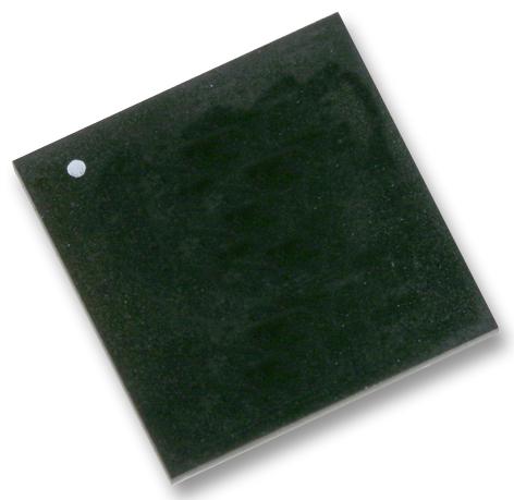
MT41K512M16VRP-107 IT:P
DRAM, DDR3L, 8 Gbit, 512M x 16bit, 933 MHz, TFBGA, 96 Pins
MT41K512M16VRP-107 IT:P is a TwinDie 1.35V automotive DDR3L SDRAM. It is a high-speed, CMOS dynamic random access memory device internally configured as two 8-bank DDR3L SDRAM devices. The DDR3L SDRAM uses a double data rate architecture to achieve high-speed operation. The double data rate architecture is an 8n-prefetch architecture with an interface designed to transfer two data words per clock cycle at the I/O balls. A single read or write access consists of a single 8n-bit-wide, one-clock-cycle data transfer at the internal DRAM core and eight corresponding n-bit-wide, one-half-clock-cycle data transfers at the I/O balls. The DDR3 SDRAM operates from a differential clock (CK and CK#). The crossing of CK going HIGH and CK# going LOW is referred to as the positive edge of CK. Control, command, and address signals are registered at every positive edge of CK.
- Backward compatible to VDD = VDDQ = 1.5V ±0.075V
- Differential bidirectional data strobe, 8n-bit prefetch architecture
- Nominal and dynamic on-die termination (ODT) for data, strobe, and mask signals
- Programmable CAS (READ) latency (CL), programmable posted CAS additive latency (AL)
- Fixed burst length (BL) of 8 and burst chop (BC) of 4 (via the mode register set [MRS])
- Self refresh temperature (SRT), automatic self refresh (ASR), write levelling
- AEC-Q100, PPAP submission, 8D response time
- 96-ball FBGA package
- Industrial temperature range from -40°C = TC = +95°C
- 1.07ns at CL = 13 (DDR3-1866) cycle time, 512 Meg x 16 configuration
Technical Attributes
Find Similar Parts
| Description | Value | |
|---|---|---|
| 933 MHz | ||
| DDR3L | ||
| TFBGA | ||
| Surface Mount | ||
| 512M x 16bit | ||
| 8 Gbit | ||
| 96 | ||
| 95 °C | ||
| -40 °C | ||
| 1.35 V |
ECCN / UNSPSC / COO
| Description | Value |
|---|---|
| Country of Origin: | null |
| ECCN: | EAR99 |
| HTSN: | 8542320032 |
| Schedule B: | null |

