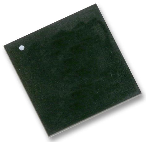
IS43DR16320C-25DBLI
DRAM Chip DDR2 DRAM 512M-Bit 32MX16 1.8V 84-Pin TWBGA
ISSI's 512Mb DDR2 SDRAM uses a double-data-ratearchitecture to achieve high-speed operation. Thedouble-data rate architecture is essentially a 4n-prefetcharchitecture, with an interface designed to transfer twodata words per clock cycle at the I/O balls.
- Vdd = 1.8V ±0.1V, Vddq = 1.8V ±0.1V
- JEDEC standard 1.8V I/O (SSTL_18-compatible)
- Double data rate interface: two data transfers per clock cycle
- Differential data strobe (DQS, DQS)
- 4-bit prefetch architecture
- On chip DLL to align DQ and DQS transitions with CK
- 4 internal banks for concurrent operation
- Programmable CAS latency (CL) 3, 4, 5, and 6 supported
- Posted CAS and programmable additive latency (AL) 0, 1, 2, 3, 4, and 5 supported
- WRITE latency = READ latency - 1 tCK
- Programmable burst lengths: 4 or 8
- Adjustable data-output drive strength, full and reduced strength options
- On-die termination (ODT)
Technical Attributes
Find Similar Parts
| Description | Value | |
|---|---|---|
| 13 Bit | ||
| 400 MHz | ||
| 16 Bit | ||
| 512 Mbit | ||
| DDR2 DRAM | ||
| 260 | ||
| 400 MHz | ||
| 360 mA | ||
| 0.4 ns | ||
| 512 Mbit | ||
| Surface Mount | ||
| 84 | ||
| 4 | ||
| 16 Bit | ||
| 16 Bit | ||
| 1.8 V | ||
| -40 to 85 °C | ||
| 85 °C | ||
| -40 °C | ||
| 32M x 16 | ||
| 84TWBGA | ||
| 84 | ||
| 12.5 x 8 x 0.8(Max) | ||
| Industrial | ||
| TWBGA | ||
| 1.8 V | ||
| DDR2 DRAM |
ECCN / UNSPSC / COO
| Description | Value |
|---|---|
| Country of Origin: | null |
| ECCN: | EAR99 |
| HTSN: | PARTS... |
| Schedule B: | PARTS... |

