
GS864032GT-200I
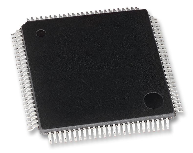
SRAM Chip Sync Quad 2.5V/3.3V 64M-Bit 2M x 32 7.5ns/3ns 100-Pin TQFP Tray
-
 RoHS 10 Compliant
 -
 Tariff Charges
The GS864032GT is a 75,497,472-bit high performance synchronous SRAM with a 2-bit burst address counter. Although of a type originally developed for Level 2 Cache applications supporting high performance CPUs, the device now finds application in synchronous SRAM applications, ranging from DSP main store to networking chip set support.Controls :Addresses, data I/Os, chip enables (E1, E2, E3), address burst control inputs (ADSP, ADSC, ADV), and write control inputs (Bx, BW, GW) are synchronous and are controlled by a positive-edge-triggered clock input (CK). Output enable (G) and power down control (ZZ) are asynchronous inputs. Burst cycles can be initiated with either ADSP or ADSC inputs. In Burst mode, subsequent burst addresses are generated internally and are controlled by ADV. The burst address counter may be configured to count in either linear or interleave order with the Linear Burst Order (LBO) input. The Burst function need not be used. New addresses can be loaded on every cycle with no degradation of chip performance.Flow Through/Pipeline Reads :The function of the Data Output register can be controlled by the user via the FT mode pin (Pin 14). Holding the FT mode pin low places the RAM in Flow Through mode, causing output data to bypass the Data Output Register. Holding FT high places the RAM in Pipeline mode, activating the rising edge-triggered Data Output Register.Byte Write and Global Write :Byte write operation is performed by using Byte Write enable (BW) input combined with one or more individual byte write signals (Bx). In addition, Global Write (GW) is available for writing all bytes at one time, regardless of the Byte Write control inputs.Sleep Mode :Low power (Sleep mode) is attained through the assertion (High) of the ZZ signal, or by stopping the clock (CK). Memory data is retained during Sleep mode.Core and Interface Voltages :The GS864032GT operates on a 2.5 V or 3.3 V power supply. All input are 3.3 V and 2.5 V compatible. Separate output po
- FT pin for user-configurable flow through or pipeline operation
- Single Cycle Deselect (SCD) operation
- 2.5 V or 3.3 V +10%/–10% core power supply
- 2.5 V or 3.3 V I/O supply
- LBO pin for Linear or Interleaved Burst mode
- Internal input resistors on mode pins allow floating mode pins
- Default to Interleaved Pipeline mode
- Byte Write (BW) and/or Global Write (GW) operation
- Internal self-timed write cycle
- Automatic power-down for portable applications
- JEDEC-standard 100-lead TQFP package
- RoHS-compliant 100-lead TQFP package available
Technical Attributes
Find Similar Parts
| Description | Value | |
|---|---|---|
| 21 Bit | ||
| Flow-Through|Pipelined | ||
| 200 MHz | ||
| SDR | ||
| 64 Mbit | ||
| Matte Tin | ||
| 260 | ||
| 250@Flow-Through|330@Pipelined mA | ||
| 2.7, 3.6 V | ||
| 7.5@Flow-Through|3@Pipelined ns | ||
| 64 Mbit | ||
| 2.3, 3 V | ||
| Surface Mount | ||
| MSL 3 - 168 hours | ||
| 100 | ||
| 32 Bit | ||
| 32 Bit | ||
| 4 | ||
| 2 MWords | ||
| -40 to 85 °C | ||
| 85 °C | ||
| -40 °C | ||
| 100TQFP | ||
| 100 | ||
| 20 x 14 x 1.4 mm | ||
| No | ||
| Industrial | ||
| Synchronous SRAM | ||
| TQFP | ||
| 2.7, 3.6 V | ||
| 2.3, 3 V | ||
| 2.5, 3.3 V | ||
| Synchronous | ||
| 2.5, 3.3 V |
ECCN / UNSPSC / COO
| Description | Value |
|---|---|
| Country of Origin: | null |
| ECCN: | 3A991.b.2.b |
| HTSN: | 8542320041 |
| Schedule B: | 8542320040 |